JAJSJF5C April   2021  – November 2024 DP83TC812R-Q1 , DP83TC812S-Q1

PRODUCTION DATA  

  1.   1
  2. 特長
  3. アプリケーション
  4. 概要
  5. Device Comparison Table
  6. Pin Configuration and Functions
  7. Specifications
    1. 6.1 Absolute Maximum Ratings
    2. 6.2 ESD Ratings
    3. 6.3 Recommended Operating Conditions
    4. 6.4 Thermal Information
    5. 6.5 Electrical Characteristics
    6. 6.6 Timing Requirements
    7. 6.7 Timing Diagrams
    8. 6.8 Typical Characteristics
  8. Detailed Description
    1. 7.1 Overview
    2. 7.2 Functional Block Diagram
    3. 7.3 Feature Description
      1. 7.3.1 Diagnostic Tool Kit
        1. 7.3.1.1 Signal Quality Indicator
        2. 7.3.1.2 Electrostatic Discharge Sensing
        3. 7.3.1.3 Time Domain Reflectometry
        4. 7.3.1.4 Voltage Sensing
        5. 7.3.1.5 BIST and Loopback Modes
          1. 7.3.1.5.1 Data Generator and Checker
          2. 7.3.1.5.2 xMII Loopback
          3. 7.3.1.5.3 PCS Loopback
          4. 7.3.1.5.4 Digital Loopback
          5. 7.3.1.5.5 Analog Loopback
          6. 7.3.1.5.6 Reverse Loopback
      2. 7.3.2 Compliance Test Modes
        1. 7.3.2.1 Test Mode 1
        2. 7.3.2.2 Test Mode 2
        3. 7.3.2.3 Test Mode 4
        4. 7.3.2.4 Test Mode 5
    4. 7.4 Device Functional Modes
      1. 7.4.1  Power Down
      2. 7.4.2  Reset
      3. 7.4.3  Standby
      4. 7.4.4  Normal
      5. 7.4.5  Sleep Ack
      6. 7.4.6  Sleep Request
      7. 7.4.7  Sleep Fail
      8. 7.4.8  Sleep
      9. 7.4.9  Wake-Up
      10. 7.4.10 TC10 System Example
      11. 7.4.11 Media Dependent Interface
        1. 7.4.11.1 100BASE-T1 Master and 100BASE-T1 Slave Configuration
        2. 7.4.11.2 Auto-Polarity Detection and Correction
        3. 7.4.11.3 Jabber Detection
        4. 7.4.11.4 Interleave Detection
      12. 7.4.12 MAC Interfaces
        1. 7.4.12.1 Media Independent Interface
        2. 7.4.12.2 Reduced Media Independent Interface
        3. 7.4.12.3 Reduced Gigabit Media Independent Interface
        4. 7.4.12.4 Serial Gigabit Media Independent Interface
      13. 7.4.13 Serial Management Interface
        1. 7.4.13.1 Direct Register Access
        2. 7.4.13.2 Extended Register Space Access
        3. 7.4.13.3 Write Operation (No Post Increment)
        4. 7.4.13.4 Read Operation (No Post Increment)
        5. 7.4.13.5 Write Operation (Post Increment)
        6. 7.4.13.6 Read Operation (Post Increment)
    5. 7.5 Programming
      1. 7.5.1 Strap Configuration
      2. 7.5.2 LED Configuration
      3. 7.5.3 PHY Address Configuration
    6. 7.6 Register Maps
      1. 7.6.1 Register Access Summary
      2. 7.6.2 DP83TC812 Registers
  9. Application and Implementation
    1. 8.1 アプリケーション情報に関する免責事項
    2. 8.2 Application Information
    3. 8.3 Typical Applications
      1. 8.3.1 Design Requirements
        1. 8.3.1.1 Physical Medium Attachment
          1. 8.3.1.1.1 Common-Mode Choke Recommendations
      2. 8.3.2 Detailed Design Procedure
      3. 8.3.3 Application Curves
    4. 8.4 Power Supply Recommendations
    5. 8.5 Layout
      1. 8.5.1 Layout Guidelines
        1. 8.5.1.1 Signal Traces
        2. 8.5.1.2 Return Path
        3. 8.5.1.3 Metal Pour
        4. 8.5.1.4 PCB Layer Stacking
      2. 8.5.2 Layout Example
  10. Device and Documentation Support
    1. 9.1 Receiving Notification of Documentation Updates
    2. 9.2 サポート・リソース
    3. 9.3 Community Resources
    4. 9.4 Trademarks
    5. 9.5 静電気放電に関する注意事項
    6. 9.6 用語集
  11. 10Revision History
  12. 11Mechanical, Packaging, and Orderable Information

パッケージ・オプション

メカニカル・データ(パッケージ|ピン)
サーマルパッド・メカニカル・データ
発注情報

LED Configuration

The DP83TC812S-Q1 supports up to three configurable Light Emitting Diode (LED) pins: LED_0, LED_1, and LED_2 (CLKOUT). Several functions can be multiplexed onto the LEDs for different modes of operation. LED operations are selected using registers 0x0450.

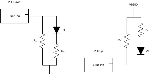
Because the LED output pins are also used as strap pins, external components required for strapping and the user must consider the LED usage to avoid contention. Specifically, when the LED outputs are used to drive LEDs directly, the active state of each output driver is dependent on the logic level sampled by the corresponding input upon power up or hardware reset.

Figure 7-19 shows the two proper ways of connecting LEDs directly to the DP83TC812S-Q1 .
DP83TC812S-Q1 DP83TC812R-Q1 Example Strap ConnectionsFigure 7-19 Example Strap Connections