JAJSJF3 December   2021 DP83TC814R-Q1 , DP83TC814S-Q1

PRODUCTION DATA  

  1. 特長
  2. アプリケーション
  3. 概要
  4. Revision History
  5. Device Comparison Table
  6. Pin Configuration and Functions
  7. Specifications
    1. 7.1 Absolute Maximum Ratings
    2. 7.2 ESD Ratings
    3. 7.3 Recommended Operating Conditions
    4. 7.4 Thermal Information
    5. 7.5 Electrical Characteristics
    6. 7.6 Timing Requirements
    7. 7.7 Timing Diagrams
    8. 7.8 Typical Characteristics
  8. Detailed Description
    1. 8.1 Overview
    2. 8.2 Functional Block Diagram
    3. 8.3 Feature Description
      1. 8.3.1 Diagnostic Tool Kit
        1. 8.3.1.1 Signal Quality Indicator
        2. 8.3.1.2 Electrostatic Discharge Sensing
        3. 8.3.1.3 Time Domain Reflectometry
        4. 8.3.1.4 Voltage Sensing
        5. 8.3.1.5 BIST and Loopback Modes
          1. 8.3.1.5.1 Data Generator and Checker
          2. 8.3.1.5.2 xMII Loopback
          3. 8.3.1.5.3 PCS Loopback
          4. 8.3.1.5.4 Digital Loopback
          5. 8.3.1.5.5 Analog Loopback
          6. 8.3.1.5.6 Reverse Loopback
      2. 8.3.2 Compliance Test Modes
        1. 8.3.2.1 Test Mode 1
        2. 8.3.2.2 Test Mode 2
        3. 8.3.2.3 Test Mode 4
        4. 8.3.2.4 Test Mode 5
    4. 8.4 Device Functional Modes
      1. 8.4.1  Power Down
      2. 8.4.2  Reset
      3. 8.4.3  Standby
      4. 8.4.4  Normal
      5. 8.4.5  Media Dependent Interface
        1. 8.4.5.1 100BASE-T1 Master and 100BASE-T1 Slave Configuration
        2. 8.4.5.2 Auto-Polarity Detection and Correction
        3. 8.4.5.3 Jabber Detection
        4. 8.4.5.4 Interleave Detection
      6. 8.4.6  MAC Interfaces
        1. 8.4.6.1 Media Independent Interface
        2. 8.4.6.2 Reduced Media Independent Interface
        3. 8.4.6.3 Reduced Gigabit Media Independent Interface
      7. 8.4.7  Serial Management Interface
      8. 8.4.8  Direct Register Access
      9. 8.4.9  Extended Register Space Access
      10. 8.4.10 Write Address Operation
        1. 8.4.10.1 MMD1 - Write Address Operation
      11. 8.4.11 Read Address Operation
        1. 8.4.11.1 MMD1 - Read Address Operation
      12. 8.4.12 Write Operation (No Post Increment)
        1. 8.4.12.1 MMD1 - Write Operation (No Post Increment)
      13. 8.4.13 Read Operation (No Post Increment)
        1. 8.4.13.1 MMD1 - Read Operation (No Post Increment)
      14. 8.4.14 Write Operation (Post Increment)
        1. 8.4.14.1 MMD1 - Write Operation (Post Increment)
      15. 8.4.15 Read Operation (Post Increment)
        1. 8.4.15.1 MMD1 - Read Operation (Post Increment)
    5. 8.5 Programming
      1. 8.5.1 Strap Configuration
      2. 8.5.2 LED Configuration
      3. 8.5.3 PHY Address Configuration
    6. 8.6 Register Maps
      1. 8.6.1 Register Access Summary
      2. 8.6.2 DP83TC814 Registers
  9. Application and Implementation
    1. 9.1 Application Information
    2. 9.2 Typical Applications
      1. 9.2.1 Design Requirements
        1. 9.2.1.1 Physical Medium Attachment
          1. 9.2.1.1.1 Common-Mode Choke Recommendations
      2. 9.2.2 Detailed Design Procedure
      3. 9.2.3 Application Curves
  10. 10Power Supply Recommendations
  11. 11Layout
    1. 11.1 Layout Guidelines
      1. 11.1.1 Signal Traces
      2. 11.1.2 Return Path
      3. 11.1.3 Metal Pour
      4. 11.1.4 PCB Layer Stacking
    2. 11.2 Layout Example
  12. 12Device and Documentation Support
    1. 12.1 Receiving Notification of Documentation Updates
    2. 12.2 サポート・リソース
    3. 12.3 Trademarks
    4. 12.4 Electrostatic Discharge Caution
    5. 12.5 Glossary
  13. 13Mechanical, Packaging, and Orderable Information

パッケージ・オプション

メカニカル・データ(パッケージ|ピン)
サーマルパッド・メカニカル・データ
発注情報

Return Path

A general best practice is to have a solid return path beneath all signal traces. This return path can be a continuous ground or DC power plane. Reducing the width of the return path can potentially affect the impedance of the signal trace. This effect is more prominent when the width of the return path is comparable to the width of the signal trace. Breaks in return path between the signal traces should be avoided at all cost. A signal crossing a split plane may cause unpredictable return path currents and could impact signal quality and result in emissions issues.
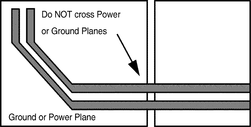
GUID-8237463F-DCD5-42D8-8A47-8397B9F39990-low.pngFigure 11-2 Power and Ground Plane Breaks