JAJSFL2H March 2016 – November 2019 DRA722 , DRA724 , DRA725 , DRA726
PRODUCTION DATA.
- 1 デバイスの概要
- 2 改訂履歴
- 3 Device Comparison
-
4 Terminal Configuration and Functions
- 4.1 Terminal Assignment
- 4.2 Ball Characteristics
- 4.3 Multiplexing Characteristics
- 4.4
Signal Descriptions
- 4.4.1 Video Input Ports (VIP)
- 4.4.2 Display Subsystem – Video Output Ports
- 4.4.3 Display Subsystem – High-Definition Multimedia Interface (HDMI)
- 4.4.4 Camera Serial Interface 2 CAL bridge (CSI2)
- 4.4.5 External Memory Interface (EMIF)
- 4.4.6 General-Purpose Memory Controller (GPMC)
- 4.4.7 Timers
- 4.4.8 Inter-Integrated Circuit Interface (I2C)
- 4.4.9 HDQ / 1-Wire Interface (HDQ1W)
- 4.4.10 Universal Asynchronous Receiver Transmitter (UART)
- 4.4.11 Multichannel Serial Peripheral Interface (McSPI)
- 4.4.12 Quad Serial Peripheral Interface (QSPI)
- 4.4.13 Multicannel Audio Serial Port (McASP)
- 4.4.14 Universal Serial Bus (USB)
- 4.4.15 SATA
- 4.4.16 Peripheral Component Interconnect Express (PCIe)
- 4.4.17 Controller Area Network Interface (DCAN)
- 4.4.18 Ethernet Interface (GMAC_SW)
- 4.4.19 Media Local Bus (MLB) Interface
- 4.4.20 eMMC/SD/SDIO
- 4.4.21 General-Purpose Interface (GPIO)
- 4.4.22 Keyboard controller (KBD)
- 4.4.23 Pulse Width Modulation (PWM) Interface
- 4.4.24 Audio Tracking Logic (ATL)
- 4.4.25 Test Interfaces
- 4.4.26 System and Miscellaneous
- 4.4.27 Power Supplies
-
5 Specifications
- 5.1 Absolute Maximum Ratings
- 5.2 ESD Ratings
- 5.3 Power-On-Hour (POH) Limits
- 5.4 Recommended Operating Conditions
- 5.5 Operating Performance Points
- 5.6 Power Consumption Summary
- 5.7
Electrical Characteristics
- 5.7.1 LVCMOS DDR DC Electrical Characteristics
- 5.7.2 HDMIPHY DC Electrical Characteristics
- 5.7.3 Dual Voltage LVCMOS I2C DC Electrical Characteristics
- 5.7.4 IQ1833 Buffers DC Electrical Characteristics
- 5.7.5 IHHV1833 Buffers DC Electrical Characteristics
- 5.7.6 LVCMOS OSC Buffers DC Electrical Characteristics
- 5.7.7 LVCMOS CSI2 DC Electrical Characteristics
- 5.7.8 BMLB18 Buffers DC Electrical Characteristics
- 5.7.9 BC1833IHHV Buffers DC Electrical Characteristics
- 5.7.10 USBPHY DC Electrical Characteristics
- 5.7.11 Dual Voltage SDIO1833 DC Electrical Characteristics
- 5.7.12 Dual Voltage LVCMOS DC Electrical Characteristics
- 5.7.13 SATAPHY DC Electrical Characteristics
- 5.7.14 PCIEPHY DC Electrical Characteristics
- 5.8 VPP Specifications for One-Time Programmable (OTP) eFuses
- 5.9 Thermal Characteristics
- 5.10 Power Supply Sequences
- 6 Clock Specifications
-
7 Timing Requirements and Switching Characteristics
- 7.1 Timing Test Conditions
- 7.2 Interface Clock Specifications
- 7.3 Timing Parameters and Information
- 7.4 Recommended Clock and Control Signal Transition Behavior
- 7.5 Virtual and Manual I/O Timing Modes
- 7.6 Video Input Ports (VIP)
- 7.7 Display Subsystem - Video Output Ports
- 7.8 Display Subsystem - High-Definition Multimedia Interface (HDMI)
- 7.9 Camera Serial Interface 2 CAL bridge (CSI2)
- 7.10 External Memory Interface (EMIF)
- 7.11 General-Purpose Memory Controller (GPMC)
- 7.12 Timers
- 7.13 Inter-Integrated Circuit Interface (I2C)
- 7.14 HDQ / 1-Wire Interface (HDQ1W)
- 7.15 Universal Asynchronous Receiver Transmitter (UART)
- 7.16 Multichannel Serial Peripheral Interface (McSPI)
- 7.17 Quad Serial Peripheral Interface (QSPI)
- 7.18 Multichannel Audio Serial Port (McASP)
- 7.19 Universal Serial Bus (USB)
- 7.20 Serial Advanced Technology Attachment (SATA)
- 7.21 Peripheral Component Interconnect Express (PCIe)
- 7.22 Controller Area Network Interface (DCAN)
- 7.23
Ethernet Interface (GMAC_SW)
- 7.23.1
GMAC MII Timings
- Table 7-70 Timing Requirements for miin_rxclk - MII Operation
- Table 7-71 Timing Requirements for miin_txclk - MII Operation
- Table 7-72 Timing Requirements for GMAC MIIn Receive 10/100 Mbit/s
- Table 7-73 Switching Characteristics Over Recommended Operating Conditions for GMAC MIIn Transmit 10/100 Mbits/s
- 7.23.2 GMAC MDIO Interface Timings
- 7.23.3
GMAC RMII Timings
- Table 7-78 Timing Requirements for GMAC REF_CLK - RMII Operation
- Table 7-79 Timing Requirements for GMAC RMIIn Receive
- Table 7-80 Switching Characteristics Over Recommended Operating Conditions for GMAC REF_CLK - RMII Operation
- Table 7-81 Switching Characteristics Over Recommended Operating Conditions for GMAC RMIIn Transmit 10/100 Mbits/s
- 7.23.4
GMAC RGMII Timings
- Table 7-85 Timing Requirements for rgmiin_rxc - RGMIIn Operation
- Table 7-86 Timing Requirements for GMAC RGMIIn Input Receive for 10/100/1000 Mbps
- Table 7-87 Switching Characteristics Over Recommended Operating Conditions for rgmiin_txctl - RGMIIn Operation for 10/100/1000 Mbit/s
- Table 7-88 Switching Characteristics for GMAC RGMIIn Output Transmit for 10/100/1000 Mbps
- 7.23.1
GMAC MII Timings
- 7.24 Media Local Bus (MLB) interface
- 7.25
eMMC/SD/SDIO
- 7.25.1
MMC1-SD Card Interface
- 7.25.1.1 Default speed, 4-bit data, SDR, half-cycle
- 7.25.1.2 High speed, 4-bit data, SDR, half-cycle
- 7.25.1.3 SDR12, 4-bit data, half-cycle
- 7.25.1.4 SDR25, 4-bit data, half-cycle
- 7.25.1.5 UHS-I SDR50, 4-bit data, half-cycle
- 7.25.1.6 UHS-I SDR104, 4-bit data, half-cycle
- 7.25.1.7 UHS-I DDR50, 4-bit data
- 7.25.2 MMC2 - eMMC
- 7.25.3 MMC3 and MMC4-SDIO/SD
- 7.25.1
MMC1-SD Card Interface
- 7.26 General-Purpose Interface (GPIO)
- 7.27 Audio Tracking Logic (ATL)
- 7.28 System and Miscellaneous interfaces
- 7.29
Test Interfaces
- 7.29.1
IEEE 1149.1 Standard-Test-Access Port (JTAG)
- 7.29.1.1
JTAG Electrical Data/Timing
- Table 7-142 Timing Requirements for IEEE 1149.1 JTAG
- Table 7-143 Switching Characteristics Over Recommended Operating Conditions for IEEE 1149.1 JTAG
- Table 7-144 Timing Requirements for IEEE 1149.1 JTAG With RTCK
- Table 7-145 Switching Characteristics Over Recommended Operating Conditions for IEEE 1149.1 JTAG With RTCK
- 7.29.1.1
JTAG Electrical Data/Timing
- 7.29.2 Trace Port Interface Unit (TPIU)
- 7.29.1
IEEE 1149.1 Standard-Test-Access Port (JTAG)
-
8 Applications, Implementation, and Layout
- 8.1 Introduction
- 8.2 Power Optimizations
- 8.3 Core Power Domains
- 8.4 Single-Ended Interfaces
- 8.5
Differential Interfaces
- 8.5.1 General Routing Guidelines
- 8.5.2
USB 2.0 Board Design and Layout Guidelines
- 8.5.2.1 Background
- 8.5.2.2
USB PHY Layout Guide
- 8.5.2.2.1 General Routing and Placement
- 8.5.2.2.2
Specific Guidelines for USB PHY Layout
- 8.5.2.2.2.1 Analog, PLL, and Digital Power Supply Filtering
- 8.5.2.2.2.2 Analog, Digital, and PLL Partitioning
- 8.5.2.2.2.3 Board Stackup
- 8.5.2.2.2.4 Cable Connector Socket
- 8.5.2.2.2.5 Clock Routings
- 8.5.2.2.2.6 Crystals/Oscillator
- 8.5.2.2.2.7 DP/DM Trace
- 8.5.2.2.2.8 DP/DM Vias
- 8.5.2.2.2.9 Image Planes
- 8.5.2.2.2.10 Power Regulators
- 8.5.2.3 References
- 8.5.3 USB 3.0 Board Design and Layout Guidelines
- 8.5.4 HDMI Board Design and Layout Guidelines
- 8.5.5 SATA Board Design and Layout Guidelines
- 8.5.6 PCIe Board Design and Layout Guidelines
- 8.5.7 CSI2 Board Design and Routing Guidelines
- 8.6 Clock Routing Guidelines
- 8.7
DDR3 Board Design and Layout Guidelines
- 8.7.1 DDR3 General Board Layout Guidelines
- 8.7.2
DDR3 Board Design and Layout Guidelines
- 8.7.2.1 Board Designs
- 8.7.2.2 DDR3 EMIF
- 8.7.2.3 DDR3 Device Combinations
- 8.7.2.4 DDR3 Interface Schematic
- 8.7.2.5 Compatible JEDEC DDR3 Devices
- 8.7.2.6 PCB Stackup
- 8.7.2.7 Placement
- 8.7.2.8 DDR3 Keepout Region
- 8.7.2.9 Bulk Bypass Capacitors
- 8.7.2.10 High Speed Bypass Capacitors
- 8.7.2.11 Net Classes
- 8.7.2.12 DDR3 Signal Termination
- 8.7.2.13 VREF_DDR Routing
- 8.7.2.14 VTT
- 8.7.2.15 CK and ADDR_CTRL Topologies and Routing Definition
- 8.7.2.16 Data Topologies and Routing Definition
- 8.7.2.17 Routing Specification
- 9 Device and Documentation Support
- 10Mechanical, Packaging, and Orderable Information
パッケージ・オプション
デバイスごとのパッケージ図は、PDF版データシートをご参照ください。
メカニカル・データ(パッケージ|ピン)
- ABC|760
サーマルパッド・メカニカル・データ
発注情報
7.16 Multichannel Serial Peripheral Interface (McSPI)
The McSPI is a master/slave synchronous serial bus. There are four separate McSPI modules (SPI1, SPI2, SPI3, and SPI4) in the device. All these four modules support up to four external devices (four chip selects) and are able to work as both master and slave.
The McSPI modules include the following main features:
- Serial clock with programmable frequency, polarity, and phase for each channel
- Wide selection of SPI word lengths, ranging from 4 to 32 bits
- Up to four master channels, or single channel in slave mode
- Master multichannel mode:
- Full duplex/half duplex
- Transmit-only/receive-only/transmit-and-receive modes
- Flexible input/output (I/O) port controls per channel
- Programmable clock granularity
- SPI configuration per channel. This means, clock definition, polarity enabling and word width
- Power management through wake-up capabilities
- Programmable timing control between chip select and external clock generation
- Built-in FIFO available for a single channel.
- Each SPI module supports multiple chip select pins spim_cs[i], where i = 1 to 4.
NOTE
For more information, see Multichannel Serial Peripheral Interface section in the device TRM.
NOTE
The McSPIm module (m = 1 to 4) is also referred to as SPIm.
CAUTION
The I/O timings provided in this section are applicable for all combinations of signals for SPI1 and SPI2. However, the timings are valid only for SPI3 and SPI4 if signals within a single IOSET are used. The IOSETS are defined in Table 7-44.
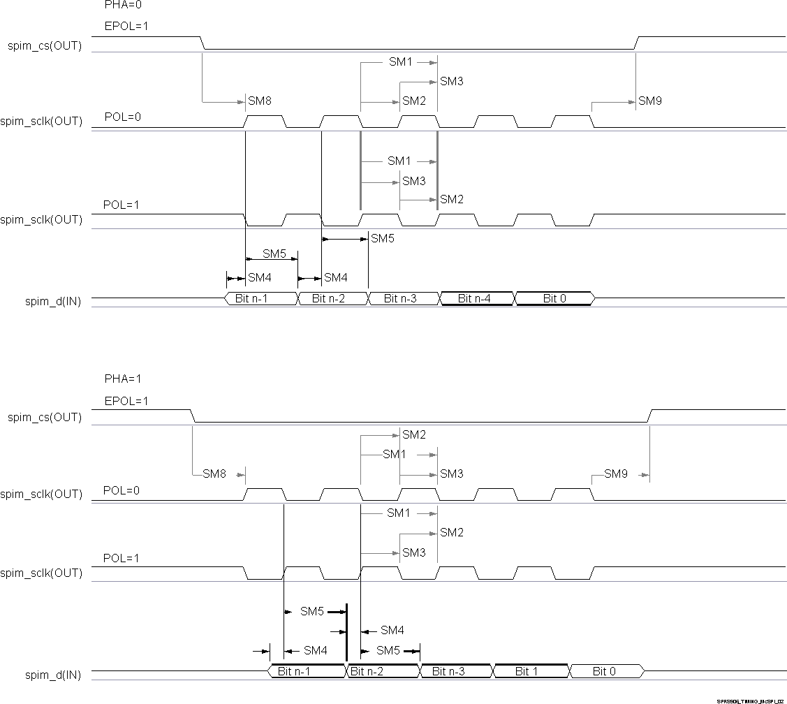
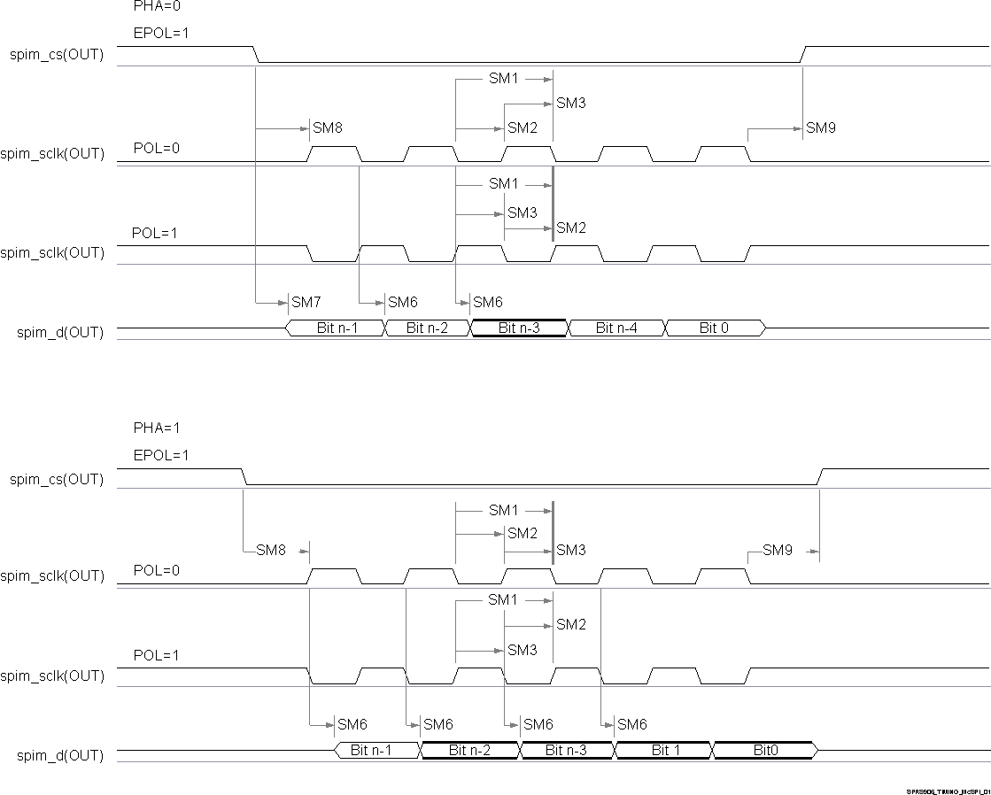
Table 7-42, Figure 7-33 and Figure 7-34 present Timing Requirements for McSPI - Master Mode.
Table 7-42 Timing Requirements for SPI - Master Mode (1)
| NO. | PARAMETER | DESCRIPTION | MODE | MIN | MAX | UNIT |
|---|---|---|---|---|---|---|
| SM1 | tc(SPICLK) | Cycle time, spi_sclk (1)(2) | SPI1/2/3/4 | 20.8 (3) | ns | |
| SM2 | tw(SPICLKL) | Typical Pulse duration, spi_sclk low (1) | 0.5 × P - 1 (4) | ns | ||
| SM3 | tw(SPICLKH) | Typical Pulse duration, spi_sclk high (1) | 0.5 × P - 1 (4) | ns | ||
| SM4 | tsu(MISO-SPICLK) | Setup time, spi_d[x] valid before spi_sclk active edge (1) | 3.5 | ns | ||
| SM5 | th(SPICLK-MISO) | Hold time, spi_d[x] valid after spi_sclk active edge (1) | 3.7 | ns | ||
| SM6 | td(SPICLK-SIMO) | Delay time, spi_sclk active edge to spi_d[x] transition (1) | SPI1 | -3.57 | 4.1 | ns |
| SPI2 | -3.9 | 3.6 | ns | |||
| SPI3 | -4.9 | 4.7 | ns | |||
| SPI4 | -4.3 | 4.5 | ns | |||
| SM7 | td(CS-SIMO) | Delay time, spi_cs[x] active edge to spi_d[x] transition | 5 | ns | ||
| SM8 | td(CS-SPICLK) | Delay time, spi_cs[x] active to spi_sclk first edge (1) | MASTER_PHA0 (5) | B - 4.2 (6) | ns | |
| MASTER_PHA1 (5) | A - 4.2 (7) | ns | ||||
| SM9 | td(SPICLK-CS) | Delay time, spi_sclk last edge to spi_cs[x] inactive (1) | MASTER_PHA0 (5) | A - 4.2 (7) | ns | |
| MASTER_PHA1 (5) | B - 4.2 (6) | ns |
- This timing applies to all configurations regardless of SPI_CLK polarity and which clock edges are used to drive output data and capture input data.
- Related to the SPI_CLK maximum frequency.
- 20.8ns cycle time = 48MHz
- P = SPICLK period.
- SPI_CLK phase is programmable with the PHA bit of the SPI_CH(i)CONF register.
- B = (TCS + 0.5) × TSPICLKREF × Fratio, where TCS is a bit field of the SPI_CH(i)CONF register and Fratio = Even ≥2.
- When P = 20.8 ns, A = (TCS + 1) × TSPICLKREF, where TCS is a bit field of the SPI_CH(i)CONF register. When P > 20.8 ns, A = (TCS + 0.5) × Fratio × TSPICLKREF, where TCS is a bit field of the SPI_CH(i)CONF register.
 Figure 7-34 McSPI - Master Mode Receive
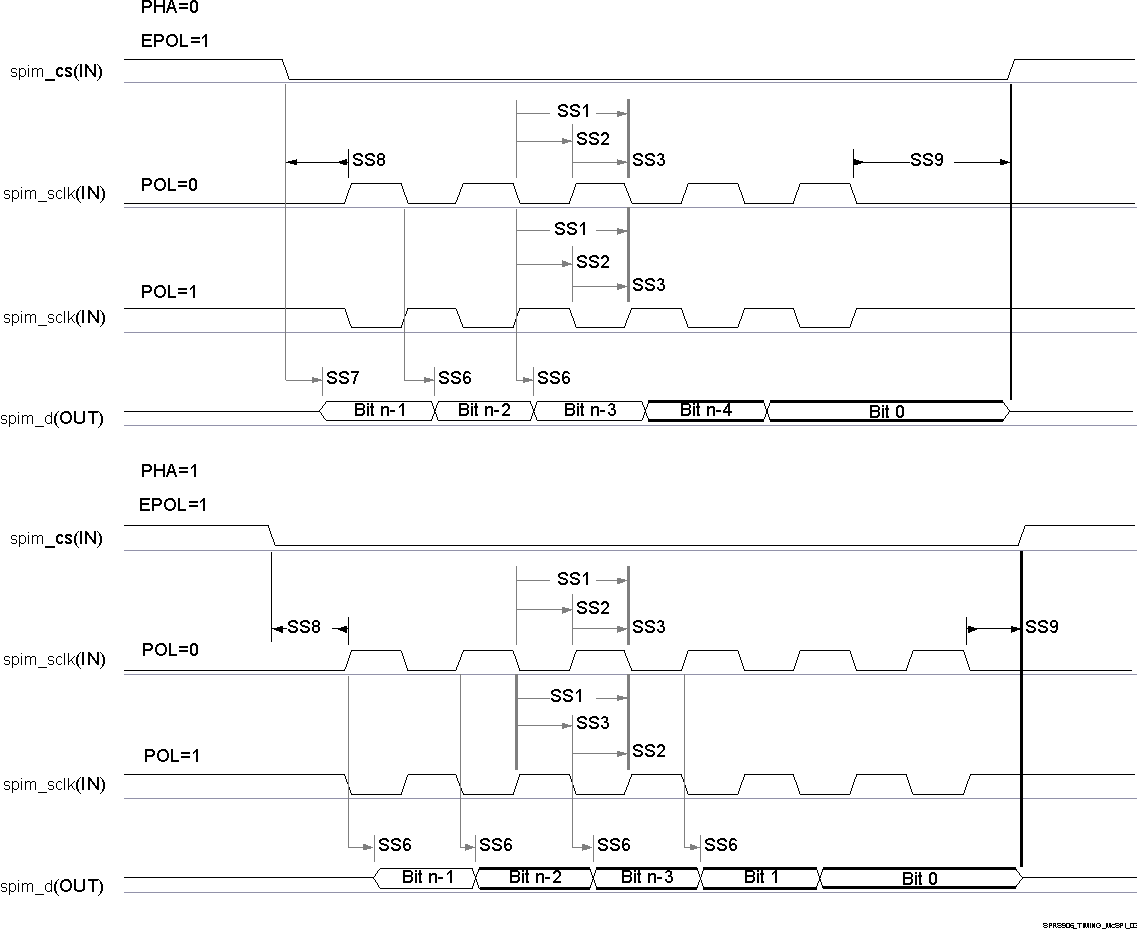
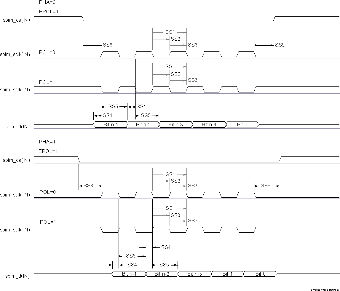
 Table 7-43, Figure 7-35 and Figure 7-36 present Timing Requirements for McSPI - Slave Mode.
Table 7-43 Timing Requirements for SPI - Slave Mode
| NO. | PARAMETER | DESCRIPTION | MODE | MIN | MAX | UNIT |
|---|---|---|---|---|---|---|
| SS1 (1) | tc(SPICLK) | Cycle time, spi_sclk | 62.5 (2)(3) | ns | ||
| SS2 (1) | tw(SPICLKL) | Typical Pulse duration, spi_sclk low | 0.45 × P (4) | ns | ||
| SS3 (1) | tw(SPICLKH) | Typical Pulse duration, spi_sclk high | 0.45 × P (4) | ns | ||
| SS4 (1) | tsu(SIMO-SPICLK) | Setup time, spi_d[x] valid before spi_sclk active edge | 5 | ns | ||
| SS5 (1) | th(SPICLK-SIMO) | Hold time, spi_d[x] valid after spi_sclk active edge | 5 | ns | ||
| SS6 (1) | td(SPICLK-SOMI) | Delay time, spi_sclk active edge to mcspi_somi transition | SPI1/2/3 | 2 | 26.6 | ns |
| SPI4 | 2 | 20.1 | ns | |||
| SS7 (5) | td(CS-SOMI) | Delay time, spi_cs[x] active edge to mcspi_somi transition | 20.95 | ns | ||
| SS8 (1) | tsu(CS-SPICLK) | Setup time, spi_cs[x] valid before spi_sclk first edge | 5 | ns | ||
| SS9 (1) | th(SPICLK-CS) | Hold time, spi_cs[x] valid after spi_sclk last edge | SPI1/2 | 5 | ns | |
| SPI3 | 7.5 | ns | ||||
| SPI4 | 6 | ns |
- This timing applies to all configurations regardless of SPI_CLK polarity and which clock edges are used to drive output data and capture input data.
- When operating the SPI interface in RX-only mode, the minimum Cycle time is 26ns (38.4MHz)
- 62.5ns Cycle time = 16 MHz
- P = SPICLK period.
- PHA = 0; SPI_CLK phase is programmable with the PHA bit of the SPI_CH(i)CONF register.
 Figure 7-35 McSPI - Slave Mode Transmit
  Figure 7-36 McSPI - Slave Mode Receive
 In Table 7-44 are presented the specific groupings of signals (IOSET) for use with SPI3 and SPI4.
Table 7-44 McSPI3/4 IOSETs
| SIGNALS | IOSET1 | IOSET2 | IOSET3 | IOSET4 | IOSET5 | |||||
|---|---|---|---|---|---|---|---|---|---|---|
| BALL | MUX | BALL | MUX | BALL | MUX | BALL | MUX | BALL | MUX | |
| McSPI3 | ||||||||||
| spi3_cs0 | D11 | 8 | V9 | 7 | A12 | 3 | D17 | 2 | AC9 | 1 |
| spi3_cs1 | B11 | 8 | AC3 | 1 | E14 | 3 | B11 | 8 | AC3 | 1 |
| spi3_cs2 | F11 | 8 | F11 | 8 | F11 | 8 | ||||
| spi3_cs3 | A10 | 8 | A10 | 8 | A10 | 8 | ||||
| spi3_d0 | C11 | 8 | W9 | 7 | B13 | 3 | G16 | 2 | AC6 | 1 |
| spi3_d1 | B10 | 8 | Y1 | 7 | A11 | 3 | A21 | 2 | AC7 | 1 |
| spi3_sclk | E11 | 8 | V2 | 7 | B12 | 3 | C18 | 2 | AC4 | 1 |
| McSPI4 | ||||||||||
| spi4_cs0 | P9 | 8 | F3 | 8 | U6 | 7 | AA4 | 2 | AB5 | 1 |
| spi4_cs1 | P4 | 8 | P4 | 8 | Y1 | 8 | Y1 | 8 | Y1 | 8 |
| spi4_cs2 | R3 | 8 | R3 | 8 | W9 | 8 | W9 | 8 | W9 | 8 |
| spi4_cs3 | T2 | 8 | T2 | 8 | V9 | 8 | V9 | 8 | V9 | 8 |
| spi4_d0 | N9 | 8 | F2 | 8 | V6 | 7 | AB3 | 2 | AB8 | 1 |
| spi4_d1 | R4 | 8 | G6 | 8 | U7 | 7 | AB9 | 2 | AD6 | 1 |
| spi4_sclk | N7 | 8 | G1 | 8 | V7 | 7 | AA3 | 2 | AC8 | 1 |
