JAJSN65A October 2019 – October 2021 DRV10982-Q1
PRODUCTION DATA
- 1 特長
- 2 アプリケーション
- 3 概要
- 4 Revision History
- 5 概要 (続き)
- 6 Pin Configuration and Functions
- 7 Specifications
-
8 Detailed Description
- 8.1 Overview
- 8.2 Functional Block Diagram
- 8.3 Feature Description
- 8.4
Device Functional Modes
- 8.4.1 Motor Parameters
- 8.4.2 Starting the Motor Under Different Initial Conditions
- 8.4.3 Motor Start Sequence
- 8.4.4 Align Current
- 8.4.5 Start-Up Current Setting
- 8.4.6 Closed Loop
- 8.4.7 Current Limit
- 8.4.8 Lock Detect and Fault Handling
- 8.4.9 Anti Voltage Suppression Function
- 8.4.10 PWM Output
- 8.4.11 FG Customized Configuration
- 8.4.12
Diagnostics and Visibility
- 8.4.12.1 Motor-Status Readback
- 8.4.12.2 Motor-Speed Readback
- 8.4.12.3 Motor Electrical-Period Readback
- 8.4.12.4 BEMF Constant Read Back
- 8.4.12.5 Motor Estimated Position by IPD
- 8.4.12.6 Supply-Voltage Readback
- 8.4.12.7 Speed-Command Readback
- 8.4.12.8 Speed-Command Buffer Readback
- 8.4.12.9 Fault Diagnostics
- 8.5
Register Maps
- 8.5.1 I2C Serial Interface
- 8.5.2 Register Map
- 8.5.3
Register Descriptions
- 8.5.3.1 FaultReg Register (address = 0x00) [reset = 0x00]
- 8.5.3.2 MotorSpeed Register (address = 0x01) [reset = 0x00]
- 8.5.3.3 MotorPeriod Register (address = 0x02) [reset = 0x00]
- 8.5.3.4 MotorKt Register (address = 0x03) [reset = 0x00]
- 8.5.3.5 MotorCurrent Register (address = 0x04) [reset = 0x00]
- 8.5.3.6 IPDPosition–SupplyVoltage Register (address = 0x05) [reset = 0x00]
- 8.5.3.7 SpeedCmd–spdCmdBuffer Register (address = 0x06) [reset = 0x00]
- 8.5.3.8 AnalogInLvl Register (address = 0x07) [reset = 0x00]
- 8.5.3.9 DeviceID–RevisionID Register (address = 0x08) [reset = 0x00]
- 8.5.3.10 DeviceID–RevisionID Register (address = 0x08) [reset = 0x00]
- 8.5.3.11 Unused Registers (addresses = 0x011 Through 0x2F)
- 8.5.3.12 SpeedCtrl Register (address = 0x30) [reset = 0x00]
- 8.5.3.13 EEPROM Programming1 Register (address = 0x31) [reset = 0x00]
- 8.5.3.14 EEPROM Programming2 Register (address = 0x32) [reset = 0x00]
- 8.5.3.15 EEPROM Programming3 Register (address = 0x33) [reset = 0x00]
- 8.5.3.16 EEPROM Programming4 Register (address = 0x34) [reset = 0x00]
- 8.5.3.17 EEPROM Programming5 Register (address = 0x35) [reset = 0x00]
- 8.5.3.18 EEPROM Programming6 Register (address = 0x36) [reset = 0x00]
- 8.5.3.19 Unused Registers (addresses = 0x37 Through 0x5F)
- 8.5.3.20 EECTRL Register (address = 0x60) [reset = 0x00]
- 8.5.3.21 Unused Registers (addresses = 0x61 Through 0x8F)
- 8.5.3.22 CONFIG1 Register (address = 0x90) [reset = 0x00]
- 8.5.3.23 CONFIG2 Register (address = 0x91) [reset = 0x00]
- 8.5.3.24 CONFIG3 Register (address = 0x92) [reset = 0x00]
- 8.5.3.25 CONFIG4 Register (address = 0x93) [reset = 0x00]
- 8.5.3.26 CONFIG5 Register (address = 0x94) [reset = 0x00]
- 8.5.3.27 CONFIG6 Register (address = 0x95) [reset = 0x00]
- 8.5.3.28 CONFIG7 Register (address = 0x96) [reset = 0x00]
- 9 Application and Implementation
- 10Power Supply Recommendations
- 11Layout
- 12Device and Documentation Support
- 13Mechanical, Packaging, and Orderable Information
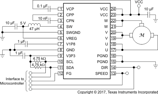
9.2 Typical Application
 Figure 9-1 Typical Application Schematic