JAJSN65A October 2019 – October 2021 DRV10982-Q1
PRODUCTION DATA
- 1 特長
- 2 アプリケーション
- 3 概要
- 4 Revision History
- 5 概要 (続き)
- 6 Pin Configuration and Functions
- 7 Specifications
-
8 Detailed Description
- 8.1 Overview
- 8.2 Functional Block Diagram
- 8.3 Feature Description
- 8.4
Device Functional Modes
- 8.4.1 Motor Parameters
- 8.4.2 Starting the Motor Under Different Initial Conditions
- 8.4.3 Motor Start Sequence
- 8.4.4 Align Current
- 8.4.5 Start-Up Current Setting
- 8.4.6 Closed Loop
- 8.4.7 Current Limit
- 8.4.8 Lock Detect and Fault Handling
- 8.4.9 Anti Voltage Suppression Function
- 8.4.10 PWM Output
- 8.4.11 FG Customized Configuration
- 8.4.12
Diagnostics and Visibility
- 8.4.12.1 Motor-Status Readback
- 8.4.12.2 Motor-Speed Readback
- 8.4.12.3 Motor Electrical-Period Readback
- 8.4.12.4 BEMF Constant Read Back
- 8.4.12.5 Motor Estimated Position by IPD
- 8.4.12.6 Supply-Voltage Readback
- 8.4.12.7 Speed-Command Readback
- 8.4.12.8 Speed-Command Buffer Readback
- 8.4.12.9 Fault Diagnostics
- 8.5
Register Maps
- 8.5.1 I2C Serial Interface
- 8.5.2 Register Map
- 8.5.3
Register Descriptions
- 8.5.3.1 FaultReg Register (address = 0x00) [reset = 0x00]
- 8.5.3.2 MotorSpeed Register (address = 0x01) [reset = 0x00]
- 8.5.3.3 MotorPeriod Register (address = 0x02) [reset = 0x00]
- 8.5.3.4 MotorKt Register (address = 0x03) [reset = 0x00]
- 8.5.3.5 MotorCurrent Register (address = 0x04) [reset = 0x00]
- 8.5.3.6 IPDPosition–SupplyVoltage Register (address = 0x05) [reset = 0x00]
- 8.5.3.7 SpeedCmd–spdCmdBuffer Register (address = 0x06) [reset = 0x00]
- 8.5.3.8 AnalogInLvl Register (address = 0x07) [reset = 0x00]
- 8.5.3.9 DeviceID–RevisionID Register (address = 0x08) [reset = 0x00]
- 8.5.3.10 DeviceID–RevisionID Register (address = 0x08) [reset = 0x00]
- 8.5.3.11 Unused Registers (addresses = 0x011 Through 0x2F)
- 8.5.3.12 SpeedCtrl Register (address = 0x30) [reset = 0x00]
- 8.5.3.13 EEPROM Programming1 Register (address = 0x31) [reset = 0x00]
- 8.5.3.14 EEPROM Programming2 Register (address = 0x32) [reset = 0x00]
- 8.5.3.15 EEPROM Programming3 Register (address = 0x33) [reset = 0x00]
- 8.5.3.16 EEPROM Programming4 Register (address = 0x34) [reset = 0x00]
- 8.5.3.17 EEPROM Programming5 Register (address = 0x35) [reset = 0x00]
- 8.5.3.18 EEPROM Programming6 Register (address = 0x36) [reset = 0x00]
- 8.5.3.19 Unused Registers (addresses = 0x37 Through 0x5F)
- 8.5.3.20 EECTRL Register (address = 0x60) [reset = 0x00]
- 8.5.3.21 Unused Registers (addresses = 0x61 Through 0x8F)
- 8.5.3.22 CONFIG1 Register (address = 0x90) [reset = 0x00]
- 8.5.3.23 CONFIG2 Register (address = 0x91) [reset = 0x00]
- 8.5.3.24 CONFIG3 Register (address = 0x92) [reset = 0x00]
- 8.5.3.25 CONFIG4 Register (address = 0x93) [reset = 0x00]
- 8.5.3.26 CONFIG5 Register (address = 0x94) [reset = 0x00]
- 8.5.3.27 CONFIG6 Register (address = 0x95) [reset = 0x00]
- 8.5.3.28 CONFIG7 Register (address = 0x96) [reset = 0x00]
- 9 Application and Implementation
- 10Power Supply Recommendations
- 11Layout
- 12Device and Documentation Support
- 13Mechanical, Packaging, and Orderable Information
8.3.3 Motor Speed Control
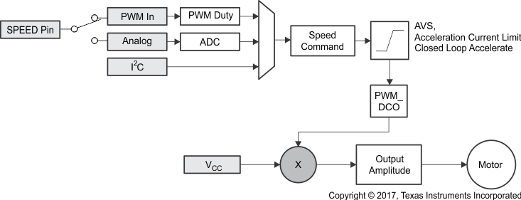
The DRV10982-Q1 device offers four methods for indirectly controlling the speed of the motor by adjusting the output voltage amplitude. This can be accomplished by varying the supply voltage (VCC) or by controlling the speed command. The speed command can be controlled in one of three ways. The user can set the speed command by adjusting either the PWM input (PWM in) or the analog input (Analog) or by writing the speed command directly through the I2C serial port (I2C). The speed command is used to determine the PWM duty cycle output (PWM_DCO) (see #SLVSCP27841).
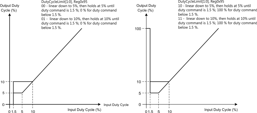
The input PWM input (PWM in) can have a minimum duty cycle limit applied. DutyCycleLimit[1:0], accessible through the I2C interface, allows the user to configure the minimum duty cycle behavior. This behavior is illustrated in #SLVSD145515.
 Figure 8-2 Duty Cycle Profile
The speed command may not always be equal to the PWM_DCO because the DRV10982-Q1 device has the AVS function (see GUID-B63F729D-F85C-4AFE-8236-14836EB4DF7F.html#GUID-B63F729D-F85C-4AFE-8236-14836EB4DF7F), the acceleration current-limit function (see GUID-D3713801-62CD-428B-B5AC-5E1FDC9A0716.html#GUID-D3713801-62CD-428B-B5AC-5E1FDC9A0716), and the closed-loop accelerate function (see GUID-B89F5D50-4AC6-4174-8132-2E3C633E0D94.html#GUID-B89F5D50-4AC6-4174-8132-2E3C633E0D94) to optimize the control performance. These functions can limit the PWM_DCO, which affects the output amplitude (see #SLVSCP27841).
 Figure 8-3 Multiplexing the Speed Command to the Output Amplitude Applied to the Motor
The output voltage amplitude applied to the motor is developed through sine wave modulation so that the phase-to-phase voltage is sinusoidal.
When any phase is measured with respect to ground, the waveform is sinusoidally coupled with third-order harmonics. This encoding technique permits one phase to be held at ground while the other two phases are pulse-width modulated. #SLVSCP23080 and #SLVSCP25769 show the sinusoidal encoding technique used in the DRV10982-Q1 device.
 Figure 8-4 PWM Output and the Average Value
| Sinusoidal voltage from phase to phase | Sinusoidal voltage with third-order harmonics from phase to GND |
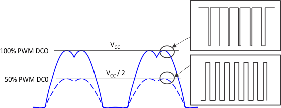
The output amplitude is determined by the magnitude of VCC and the PWM duty cycle output (PWM_DCO). The PWM_DCO represents the peak duty cycle that is applied in one electrical cycle. The maximum amplitude is reached when PWM_DCO is at 100%. The peak output amplitude is VCC. When the PWM_DCO is at 50%, the peak amplitude is VCC / 2 (see #SLVSCP29325).
 Figure 8-6 Output Voltage Amplitude Adjustment
Motor speed is controlled indirectly by controlling the output amplitude, which is achieved by either controlling VCC, or controlling the PWM_DCO. The DRV10982-Q1 device provides different options for the user to control the PWM_DCO:
- Analog input (SPEED pin)
- PWM encoded digital input (SPEED pin)
- I2C serial interface.
See the GUID-89327AFF-5A52-4E52-A5BF-A5C78660B095.html#GUID-89327AFF-5A52-4E52-A5BF-A5C78660B095 section for more information.