SLVSB25C August 2011 – June 2015 DRV201
PRODUCTION DATA.
- 1 Features
- 2 Applications
- 3 Description
- 4 Revision History
- 5 Pin Configuration and Functions
- 6 Specifications
-
7 Detailed Description
- 7.1 Overview
- 7.2 Functional Block Diagram
- 7.3 Feature Description
- 7.4 Device Functional Modes
- 7.5 Programming
- 7.6
Register Maps
- 7.6.1 Register Address Map
- 7.6.2 Control Register (Control) Address - 0x02h
- 7.6.3 VCM MSB Current Control Register (VCM_Current_MSB) Address - 0x03h
- 7.6.4 VCM LSB Current Control Register (VCM_Current_LSB) Address - 0x04h
- 7.6.5 Status Register (Status) Address - 0x05h
- 7.6.6 Mode Register (Mode) Address - 0x06h
- 7.6.7 VCM Resonance Frequency Register (VCM_FREQ) Address - 0x07h
- 8 Application and Implementation
- 9 Power Supply Recommendations
- 10Layout
- 11Device and Documentation Support
- 12Mechanical, Packaging, and Orderable Information
パッケージ・オプション
メカニカル・データ(パッケージ|ピン)
サーマルパッド・メカニカル・データ
発注情報
10 Layout
10.1 Layout Guidelines
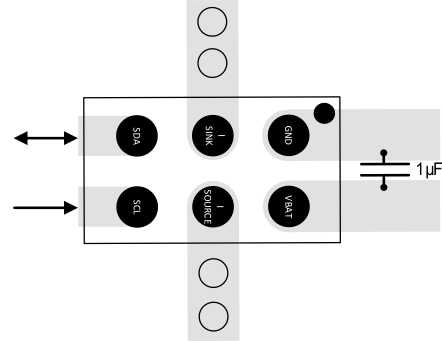
The VBAT pin should be bypassed to GND using a low-ESR ceramic bypass capacitor with a recommended value of at least 1-µF rated for a minimum of 6.3 V. Place this capacitor as close to the VBAT and GND pins as possible with a thick trace or ground plane connection to the device GND pin.
10.2 Layout Example
 Figure 26. Recommended Layout Example