JAJSCC7D June   2016  – November 2023 DRV2510-Q1

PRODUCTION DATA  

  1.   1
  2. 特長
  3. アプリケーション
  4. 概要
  5. Revision History
  6. Pin Configuration and Functions
  7. Specifications
    1. 6.1 Absolute Maximum Ratings
    2. 6.2 ESD Ratings
    3. 6.3 Recommended Operating Conditions
    4. 6.4 Thermal Information
    5. 6.5 Electrical Characteristics
    6. 6.6 Timing Requirements
    7. 6.7 Switching Characteristics
    8. 6.8 Typical Characteristics
  8. Detailed Description
    1. 7.1 Overview
    2. 7.2 Functional Block Diagram
    3. 7.3 Feature Description
      1. 7.3.1 Analog Input and Configurable Pre-amplifier
      2. 7.3.2 Pulse-Width Modulator (PWM)
      3. 7.3.3 Designed for low EMI
      4. 7.3.4 Device Protection Systems
        1. 7.3.4.1 Diagnostics
          1. 7.3.4.1.1 Load Diagnostics
        2. 7.3.4.2 Faults During Load Diagnostics
        3. 7.3.4.3 Protection and Monitoring
    4. 7.4 Device Functional Modes
      1. 7.4.1 Operation in Shutdown Mode
      2. 7.4.2 Operation in Standby Mode
      3. 7.4.3 Operation in Active Mode
    5. 7.5 Programming
      1. 7.5.1 General I2C Operation
      2. 7.5.2 Single-Byte and Multiple-Byte Transfers
      3. 7.5.3 Single-Byte Write
      4. 7.5.4 Multiple-Byte Write and Incremental Multiple-Byte Write
      5. 7.5.5 Single-Byte Read
      6. 7.5.6 Multiple-Byte Read
    6. 7.6 Register Map
      1. 7.6.1 Address: 0x01
      2. 7.6.2 Address: 0x02
      3. 7.6.3 Address: 0x03
  9. Application and Implementation
    1. 8.1 Application Information
    2. 8.2 Typical Applications
      1. 8.2.1 Single-Ended Source
        1. 8.2.1.1 Design Requirements
        2. 8.2.1.2 Detailed Design Procedure
          1. 8.2.1.2.1 Optional Components
          2. 8.2.1.2.2 Capacitor Selection
          3. 8.2.1.2.3 Solenoid Selection
          4. 8.2.1.2.4 Output Filter Considerations
        3. 8.2.1.3 Application Curves
        4. 8.2.1.4 Differential Input Diagram
  10. Power Supply Recommendations
  11. 10Layout
    1. 10.1 Layout Guidelines
    2. 10.2 Layout Example
  12. 11Device and Documentation Support
    1. 11.1 Device Support
      1. 11.1.1 サード・パーティ製品に関する免責事項
    2. 11.2 ドキュメントの更新通知を受け取る方法
    3. 11.3 サポート・リソース
    4. 11.4 Trademarks
    5. 11.5 静電気放電に関する注意事項
    6. 11.6 用語集
  13. 12Mechanical, Packaging, and Orderable Information

パッケージ・オプション

メカニカル・データ(パッケージ|ピン)
サーマルパッド・メカニカル・データ
発注情報
Load Diagnostics

The load diagnostic function runs on assertion of EN or when the device is in a fault state (dc detect, overcurrent, overvoltage, undervoltage, and overtemperature). During this test, the outputs are in a Hi-Z state. The device determines whether the output is a short to GND, short to VDD, open load, or shorted load. The load diagnostic biases the output, which therefore requires limiting the capacitance value for proper functioning. The load diagnostic test takes approximately 229 ms to run. Note that the check phase repeats up to five times if a fault is present or a large capacitor to GND is present on the output. On detection of an open load, the output still operates. On detection of any other fault condition, the output goes into a Hi-Z state, and the device checks the load continuously until removal of the fault condition. After detection of a normal output condition, the output starts. The load diagnostics run after every other overvoltage (OV) event. The load diagnostic for open load only has I2C reporting. All other faults have I2C and INTZ pin assertion.

The device performs load diagnostic tests as shown in Figure 7-2.

GUID-1A84CDD6-AF43-4FDF-9F04-A43D70417B88-low.gifFigure 7-2 Load Diagnostics Sequence of Events

Figure 7-3 illustrates how the diagnostics determine the load based on output conditions.
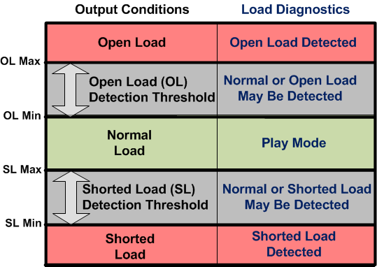
GUID-EFB0AA3D-2A5D-4F04-A09A-F497BCEB6DB6-low.gif Figure 7-3 Load Diagnostic Reporting Thresholds