SLOS754C June 2012 – August 2016 DRV2603
PRODUCTION DATA.
- 1 Features
- 2 Applications
- 3 Description
- 4 Revision History
- 5 Pin Configuration and Functions
- 6 Specifications
- 7 Parameter Measurement Information
-
8 Detailed Description
- 8.1 Overview
- 8.2 Functional Block Diagram
- 8.3
Feature Description
- 8.3.1 Supply Voltage Rejection for Constant Vibration Strength
- 8.3.2 Low-Voltage Control Logic for Constant Vibration Strength
- 8.3.3 Thermal Protection
- 8.3.4 Overcurrent Protection
- 8.3.5 Linear Resonance Actuators (LRA)
- 8.3.6 Auto Resonance Engine for LRA
- 8.3.7 Eccentric Rotating Mass Motors (ERM)
- 8.3.8 Edge Rate Control
- 8.4 Device Functional Modes
- 9 Application and Implementation
- 10Power Supply Recommendations
- 11Layout
- 12Device and Documentation Support
- 13Mechanical, Packaging, and Orderable Information
パッケージ・オプション
メカニカル・データ(パッケージ|ピン)
- RUN|10
サーマルパッド・メカニカル・データ
- RUN|10
発注情報
1 Features
- Flexible Haptic/Vibra Driver
- LRA (Linear Resonance Actuator)
- ERM (Eccentric Rotating Mass)
- Auto Resonance Tracking for LRA
- No Frequency Calibration Required
- Automatic Drive Commutation
- Automatic Braking Algorithm
- Wide Input PWM Frequency Range
- Constant Vibration Strength Over Supply
- Automatic Input Level Translation
- 0% to 100% Duty Cycle Control Range
- Fast Start Up Time
- Differential Drive from Single-Ended Input
- Wide Supply Voltage Range of 2.5 V to 5.2 V
- Immersion TouchSense® 3000 Compatible
- 1.8-V Compatible, 5-V Tolerant Digital Pins
- Available in a 2 mm × 2 mm × 0.75 mm Leadless QFN Package (RUN)
2 Applications
- Mobile Phones and Tablets
- Watches and Wearable Technology
- Remote Controls, Mice, and Peripheral Devices
- Electronic Point of Sale (ePOS)
- Vibration Alerts and Notifications
- Touch-Enabled Devices
- Industrial Human-Machine Interfaces
3 Description
The DRV2603 is a haptic driver designed specifically to solve common obstacles in driving both Linear Resonance Actuator (LRA) and Eccentric Rotating Mass (ERM) haptic elements. The DRV2603 is designed for low latency, high efficiency, and more drive strength for actuators commonly used for tactile feedback in the portable market.
LRA actuators typically have a narrow frequency band over which they have an adequate haptic response. This frequency window is typically ±2.5 Hz wide or less, so driving an LRA actuator presents a challenge. The DRV2603 solves this problem by employing auto resonance tracking, which automatically detects and tracks the LRA resonant frequency in real time. This means that any input PWM frequency within the input range (10 kHz to 250 kHz) will automatically produce the correct resonant output frequency. As an additional benefit, the DRV2603 implements an automatic braking algorithm to prevent LRA ringing at the end of waveforms, leaving the user with a crisp haptic sensation.
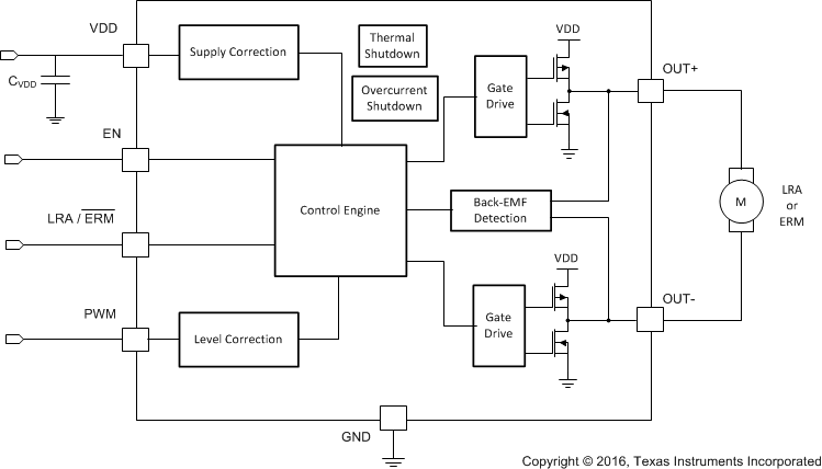
For both ERM and LRA actuators, the automatic input level translation solves issues with low voltage PWM sources without adding additional external components, so if the digital I/O levels vary, the output voltage does not change. The DRV2603 also has supply correction that ensures no supply regulation is required for constant vibration strength, allowing an efficient, direct-battery connection.
Device Information(1)
| PART NUMBER | PACKAGE | BODY SIZE (NOM) |
|---|---|---|
| DRV2603 | WQFN (10) | 2.00 mm × 2.00 mm |
- For all available packages, see the orderable addendum at the end of the datasheet.
DRV2603 Block Diagram
