JAJSC41E September 2015 – February 2017 DRV3205-Q1
PRODUCTION DATA.
- 1 特長
- 2 アプリケーション
- 3 概要
- 4 改訂履歴
- 5 Pin Configuration and Functions
- 6 Specifications
- 7 Detailed Description
- 8 Application and Implementation
- 9 Power Supply Recommendations
- 10Layout
- 11デバイスおよびドキュメントのサポート
- 12メカニカル、パッケージ、および注文情報
パッケージ・オプション
メカニカル・データ(パッケージ|ピン)
- PHP|48
サーマルパッド・メカニカル・データ
- PHP|48
発注情報
7 Detailed Description
7.1 Overview
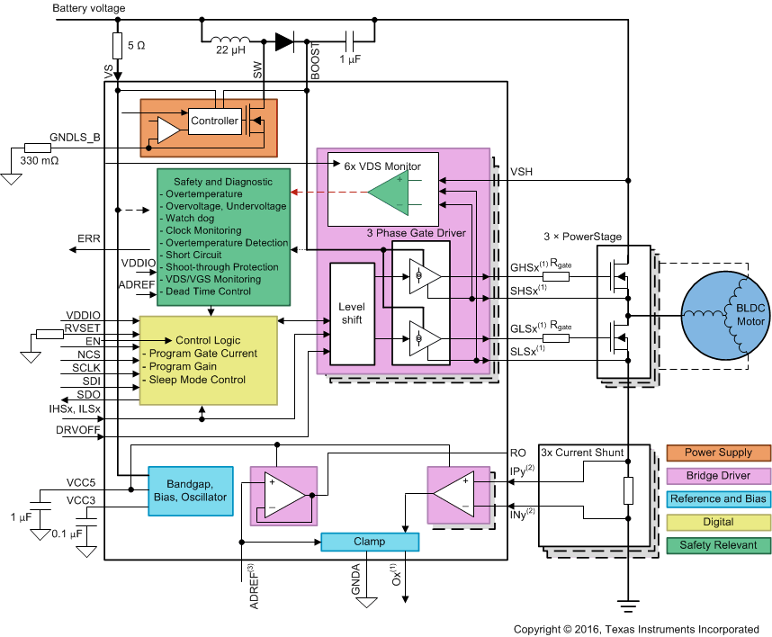
The DRV3205-Q1 is designed to control 3-phase brushless DC motors in automotive applications using pulse-width modulation. Three high-side and three low-side gate drivers can be switched individually with low propagation delay. The input logic prevents simultaneous activation of the high-side and low-side driver of the same channel. A configuration and status register can be accessed through a SPI communication interface.
7.2 Functional Block Diagram

7.3 Programming
7.3.1 SPI
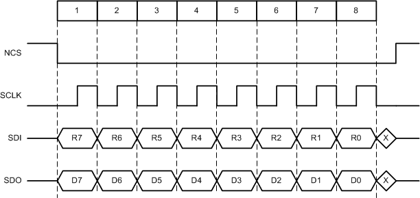
The SPI slave interface is used for serial communication with the external SPI master (external MCU). The SPI communication starts with the NCS falling edge and ends with NCS rising edge. The NCS high level keeps the SPI slave interface in reset state, and the SDO output in tri-state.
7.3.1.1 Address Mode Transfer
The address mode transfer is an 8-bit protocol. Both SPI slave and SPI master transmit the MSB first.

NOTE:
SPI master (MCU) and SPI slave (DRV3205-Q1) sample received data on the rising SCLK edge and transmit on the falling SCLK edge.After the NCS falling edge, the first word of 7 bits are address bits followed by the RW bit. During first address transfer, the device returns the STAT1 register on SDO.
Each complete 8-bit frame will be processed. If NCS goes high before a multiple of 8 bits is transferred, the bits are ignored.
7.3.1.1.1 SPI Address Transfer Phase
| Bit | D7 | D6 | D5 | D4 | D3 | D2 | D1 | D0 |
|---|---|---|---|---|---|---|---|---|
| Function | ADDR6 | ADDR5 | ADDR4 | ADDR3 | ADDR2 | ADDR1 | ADDR0 | RW |
-
ADDR [6:0] Register address
-
RW Read and write access
RW = 0: Read access. The SPI master performs a read access to selected register. During following SPI transfer, the device returns the requested register read value on SDO, and device interprets SDI bits as a next address transfer.
RW = 1: Write access. The master performs a write access on the selected register. The slave updates the register value during next SPI transfer (if followed immediately) and returns the current register value on SDO.
7.3.1.2 SPI Data Transfer Phase
| Bit | D7 | D6 | D5 | D4 | D3 | D2 | D1 | D0 |
|---|---|---|---|---|---|---|---|---|
| Function | DATA7 | DATA6 | DATA5 | DATA4 | ADDR3 | DATA2 | DATA1 | DATA0 |
-
DATA [7:0] Data value for write access (8-Bit).
Figure 8 shows data value encoding scheme during a write access. Mixing the two access modes (write and read access) during one SPI communication sequence (NCS = 0) is possible. The SPI communication can be terminated after single 8-bit SPI transfer by asserting NCS = 1. Device returns STAT1 register (for the very first SPI transfer after power-up) or current register value that was addressed during SPI Transfer Address Phase.
7.3.1.3 Device Data Response
| Bit | D7 | D6 | D5 | D4 | D3 | D2 | D1 | D0 |
|---|---|---|---|---|---|---|---|---|
| Function | REG7 | REG6 | REG5 | REG4 | REG3 | REG2 | REG1 | REG0 |
-
REG [7:0] Internal register value. All unused bits are set to 0.
Figure 10 shows a complete 16-bit SPI frame. Figure 11, Figure 12, Figure 13, Figure 14, Figure 15, and Figure 16 show the frame examples.

 Figure 11. Write Access Followed by Read Access
 Figure 12. Read Access Followed by Read Access
 Figure 13. Write Access Followed by Write Access
 Figure 14. Read Access Followed by Write Access
 Figure 15. Read Access Followed by Read Access Followed by Write Access
 Figure 16. Read Access Followed by Read Access Followed by Read Access
7.4 Register Maps
Table 1. Register Address Map
| Address | Name | Reset Value | CRC Check | Access State(1) | Reset Event(2)
(bit wide exception) |
|---|---|---|---|---|---|
| 0×01 | Configuration register 0 (CFG0) | 8'h3F | Yes | W/R : D, A([6:3]) R : A(7,[2:0], SF |
RST1-4 |
| 0×02 | Configuration register 1 (CFG1) | 8'h3F | Yes | W/R: D R: A, SF |
RST1-4 |
| 0×03 | Configuration register 2 (CFG2) | 8'h00 | Yes | W/R: D R: A, SF |
RST1-4 |
| 0×04 | HS 1/2/3 drive register (CURR0) ON | 8'h00 | Yes | W/R: D R: A, SF |
RST1-4 |
| 0×05 | LS 1/2/3 drive register (CURR1) ON | 8'h00 | Yes | W/R: D R: A, SF |
RST1-4 |
| 0×06 | HS 1/2/3 drive register (CURR2) OFF | 8'h00 | Yes | W/R: D R: A, SF |
RST1-4 |
| 0×07 | LS 1/2/3 drive register (CURR3) OFF | 8'h00 | Yes | W/R: D R: A, SF |
RST1-4 |
| 0×08 | Safety/error configuration register (SECR1) | 8'hC0 | Yes | W/R: D R: A, SF |
RST1 |
| 0×09 | Safety function configuration register (SFCR1) | 8'h80 | Yes | W/R: D R: A, SF |
RST1-3 |
| 0×0A | Status register 0 (STAT0) | 8'h00 | No | R: D, A, SF | RST1-4 |
| 0×0B | Status register 1 (STAT1) | 8'h80 | No | R: D, A, SF | RST1-3 |
| 0×0C | Status register 2 (STAT2) | 8'h00 | No | R: D, A, SF | RST1-3 |
| 0×0D | Status register 3 (STAT3) | 8'h03 | No | R: D, A, SF | RST1-3 |
| 0×0E | Status register 4 (STAT4) | 8'h00 | No | R: D, A, SF | RST1-3 |
| 0×0F | Status register 5 (STAT5) | 8'h03 | No | R: D, A, SF | RST1-3 (Bit[4]:RST1) |
| 0×10 | Status register 6 (STAT6) | 8'h00 | No | R: D, A, SF | RST1-3 |
| 0×11 | Status register 7 (STAT7) | 8'h00 | No | R: D, A, SF | RST1-4 |
| 0×12 | Status register 8 (STAT8) | 8'h00 | No | R: D, A, SF | RST1-4 (Bit[0]:RST1) |
| 0×13 | Safety error status (SAFETY_ERR_STAT) | 8'h00 | No | R: D, A, SF | RST1-3 (Bit[3:1]:RST1) |
| 0×14 | Status register 9 (STAT9) | 8'h00 | No | R: D, A, SF | RST1-3 |
| 0×15 | Reserved1 | 8'h00 | No | W/R: D, A, SF | RST1-3 |
| 0×16 | Reserved2 | 8'h00 | No | W/R: D, A, SF | RST1-3 |
| 0×1E | SPI transfer write CRC register (SPIWR_CRC) | 8'h00 | No | W/R: D, A, SF | RST1-3 |
| 0×1F | SPI transfer read CRC register (SPIRD_CRC) | 8'hFF | No | R: D, A, SF | RST1-3 |
| 0×20 | SAFETY_CHECK_CTRL register ( SFCC1) | 8'h01 | No | W/R: D R: A, SF |
RST1-3 |
| 0×21 | CRC control register (CRCCTL) | 8'h00 | No | W/R: D, A R: SF |
RST1-3 |
| 0×22 | CRC calculated (CRCCALC) | N/A | No | W/R: D R: A, SF |
RST1-3 |
| 0×23 | Reserved 3 | 8'h00 | No | W/R: D, A, SF | RST1-3 |
| 0×24 | HS/LS read back (RB0) | 8'h00 | No | R: D, A, SF | RST1-3 |
| 0×25 | HS/LS count control (RB1) | 8'h00 | No | W/R: D, A R: SF |
RST1-4 |
| 0×26 | HS/LS count (RB2) | 8'h00 | No | R: D, A, SF | RST1-4 |
| 0×27 | Configuration register 3 (CFG3) | 8'hAB | Yes | W/R: D R: A, SF |
RST1-4 |
| 0×28 | Configuration register 4 (CFG4) | 8'h00 | Yes | W/R: D R: A, SF |
RST1-4 |
| 0×29 | Configuration register 5 (CFG5) | 8'hAB | Yes | W/R: D R: A, SF |
RST1-3 |
| 0×2A | CSM unlock (CSM_UNLOCK1) | 8'h00 | No | W/R: D R: A, SF |
RST1-4 |
| 0×2B | CSM unlock (CSM_UNLOCK2) | 8'h3F | No | W/R: D R: A, SF |
RST1-4 |
| 0×2C | RO configuration register 2 (RO_CFG) | 8'h00 | Yes | W/R: D R: A, SF |
RST1-4 |
| 0×2D | Safety BIST control register 1 (SAFETY_BIST_CTL1) | 8'h00 | Yes | W/R: D R: SF, A |
RST1-3 |
| 0×2E | SPI test register (SPI_TEST) | 8'h00 | No | W/R: D, A, SF | RST1-4 |
| 0×2F | Reserved4 | 8'h00 | No | W/R: D, A, SF | RST1-3 |
| 0×30 | Safety BIST control register 2 (SAFETY_BIST_CTL2) | 8'h00 | Yes | W/R: D R: SF, A |
RST1-3 (Bit[5]:RST1) |
| 0×31 | Watch dog timer configuration register (WDT_WIN1_CFG) | 8'h02 | Yes | W/R: D R: SF, A |
RST1-4 |
| 0×32 | Watch dog timer configuration register (WDT_WIN2_CFG) | 8'h08 | Yes | W/R: D R: SF, A |
RST1-4 |
| 0×33 | Watch dog timer TOKEN register (WDT_TOKEN_FDBCK) | 8'h04 | Yes | W/R: D R: SF, A |
RST1 |
| 0×34 | Watch dog timer TOKEN register (WDT_TOKEN_VALUE) | 8'h40 | No | R: D, SF, A | RST1-4 |
| 0×35 | Watch dog timer ANSWER register (WDT_ANSWER) | 8'h00 | No | W/R: D, A, SF | RST1-4 |
| 0×36 | Watch dog timer status register (WDT_STATUS) | 8'hC0 | No | R: D, A, SG | RST1-4 |
| 0×37 | Watch dog failure detection configuration register (WD_FAIL_CFG) | 8'hEC | Yes | W/R: D R: SF, A |
RST1-4 |
| 0×38 | Configuration register 6 (CFG6) | 8'h10 | Yes | W/R: D R: A, SF |
RST1-4 |
| 0×39 | Configuration register 7 (CFG7) | 8'h13 | Yes | W/R : D R : A, SF |
RST1-4 |
| 0×3A | Configuration register 8 (CFG8) | 8'h20 | Yes | W/R : D R : A, SF |
RST1-4 |
| 0×3B | Configuration register 9 (CFG9) | 8'hFE | Yes | W/R : D R : A, SF |
RST1-4 |
D: DIAGNOSITC STATE, A: ACTIVE STATE, SF: SAFE STATE, SY: STANDBY STATE, R: RESET