JAJSEM5 February   2019 DRV5021-Q1

PRODUCTION DATA.  

  1. 特長
  2. アプリケーション
  3. 概要
    1.     Device Images
      1.      標準アプリケーション回路図
      2.      磁気応答
  4. 改訂履歴
  5. Pin Configuration and Functions
    1.     Pin Functions
  6. Specifications
    1. 6.1 Absolute Maximum Ratings
    2. 6.2 ESD Ratings
    3. 6.3 Recommended Operating Conditions
    4. 6.4 Thermal Information
    5. 6.5 Electrical Characteristics
    6. 6.6 Magnetic Characteristics
    7. 6.7 Typical Characteristics
  7. Detailed Description
    1. 7.1 Overview
    2. 7.2 Functional Block Diagram
    3. 7.3 Feature Description
      1. 7.3.1 Field Direction Definition
      2. 7.3.2 Device Output
      3. 7.3.3 Power-On Time
      4. 7.3.4 Hall Element Location
      5. 7.3.5 Propagation Delay
      6. 7.3.6 Output Stage
    4. 7.4 Device Functional Modes
  8. Application and Implementation
    1. 8.1 Application Information
    2. 8.2 Typical Applications
      1. 8.2.1 Proximity Sensing Circuit
        1. 8.2.1.1 Design Requirements
        2. 8.2.1.2 Detailed Design Procedure
          1. 8.2.1.2.1 Configuration Example
        3. 8.2.1.3 Application Curves
      2. 8.2.2 Alternative Two-Wire Application
        1. 8.2.2.1 Design Requirements
        2. 8.2.2.2 Detailed Design Procedure
  9. Power Supply Recommendations
  10. 10Layout
    1. 10.1 Layout Guidelines
    2. 10.2 Layout Example
  11. 11デバイスおよびドキュメントのサポート
    1. 11.1 ドキュメントのサポート
      1. 11.1.1 関連資料
    2. 11.2 ドキュメントの更新通知を受け取る方法
    3. 11.3 コミュニティ・リソース
    4. 11.4 商標
    5. 11.5 静電気放電に関する注意事項
    6. 11.6 Glossary
  12. 12メカニカル、パッケージ、および注文情報

パッケージ・オプション

メカニカル・データ(パッケージ|ピン)
サーマルパッド・メカニカル・データ
発注情報

Output Stage

The DRV5021-Q1 output stage uses an open-drain NMOS transistor that is rated to sink up to 20 mA of current. For proper operation, calculate the value of pullup resistor R1 using Equation 1.

Equation 1. DRV5021-Q1 drv5021-equation-1.gif

The size of R1 is a tradeoff between the OUT rise time and the current when OUT is pulled low. A lower current is generally better; however, faster transitions and bandwidth require a smaller resistor for faster switching.

In addition, the value of R1 must be > 500 Ω in order to make sure that the output driver can pull the OUT pin close to GND.

NOTE

Vref is not restricted to VCC. The allowable voltage range of this pin is specified in the Recommended Operating Conditions.
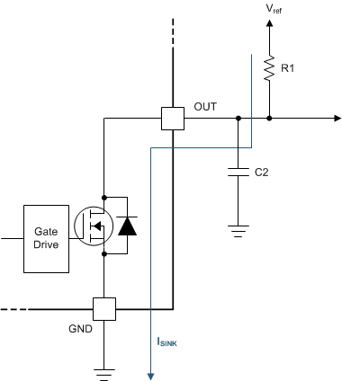
DRV5021-Q1 drv5021-open-drain-output.gifFigure 19. Open-Drain Output

Select a value for C2 based on the system bandwidth specifications shown in Equation 2.

Equation 2. DRV5021-Q1 eq_02_slis150.gif

Most applications do not require this C2 filtering capacitor.