JAJSGG8A november   2018  – august 2020 DRV5057

PRODUCTION DATA  

  1.   1
  2. 特長
  3. アプリケーション
  4. 説明
  5. Revision History
  6. Pin Configuration and Functions
    1.     Pin Functions
  7. Specifications
    1. 6.1 Absolute Maximum Ratings
    2. 6.2 ESD Ratings
    3. 6.3 Recommended Operating Conditions
    4. 6.4 Thermal Information
    5. 6.5 Electrical Characteristics
    6. 6.6 Magnetic Characteristics
    7. 6.7 Typical Characteristics
  8. Detailed Description
    1. 7.1 Overview
    2. 7.2 Functional Block Diagram
    3. 7.3 Feature Description
      1. 7.3.1 Magnetic Flux Direction
      2. 7.3.2 Sensitivity Linearity
      3. 7.3.3 Operating VCC Ranges
      4. 7.3.4 Sensitivity Temperature Compensation for Magnets
      5. 7.3.5 Power-On Time
      6. 7.3.6 Hall Element Location
    4. 7.4 Device Functional Modes
  9. Application and Implementation
    1. 8.1 Application Information
      1. 8.1.1 Selecting the Sensitivity Option
      2. 8.1.2 Decoding a PWM
        1. 8.1.2.1 Decoding a PWM (Digital)
          1. 8.1.2.1.1 Capture and Compare Timer Interrupt
          2. 8.1.2.1.2 Oversampling and Counting With a Timer Interrupt
          3. 8.1.2.1.3 Accuracy and Resolution
        2. 8.1.2.2 Decoding a PWM (Analog)
    2. 8.2 Typical Applications
      1. 8.2.1 Full-Swing Orientation Example
        1. 8.2.1.1 Design Requirements
        2. 8.2.1.2 Detailed Design Procedure
        3. 8.2.1.3 Application Curve
      2. 8.2.2 Half-Swing Orientation Example
        1. 8.2.2.1 Design Requirements
        2. 8.2.2.2 Detailed Design Procedure
    3. 8.3 What to Do and What Not to Do
  10. Power Supply Recommendations
  11. 10Layout
    1. 10.1 Layout Guidelines
    2. 10.2 Layout Examples
  12. 11Device and Documentation Support
    1. 11.1 Documentation Support
      1. 11.1.1 Related Documentation
    2. 11.2 ドキュメントの更新通知を受け取る方法
    3. 11.3 サポート・リソース
    4. 11.4 Trademarks
    5. 11.5 静電気放電に関する注意事項
    6. 11.6 用語集
  13. 12Mechanical, Packaging, and Orderable Information

パッケージ・オプション

メカニカル・データ(パッケージ|ピン)
サーマルパッド・メカニカル・データ
発注情報
Accuracy and Resolution

The accuracy and resolution for the methods described in the Section 8.1.2.1.1 and Section 8.1.2.1.2 sections depends significantly on the timer sampling frequency. Equation 2 calculates the least significant bit of the duty cycle (%DLSB) based on the chosen timer sampling frequency.

Equation 2. GUID-02E3D724-C8AA-492C-A2D8-1C9BD67FEB84-low.gif

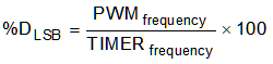
For example, with a 2-kHz PWM and a 400-kHz sampling frequency, the %DLSB is:

(2 kHz / 400 kHz) × 100 = 0.5%DLSB

If the sampling frequency in increased to 2-MHz, the %DLSB is improved to be:

(2 MHz / 400 kHz) × 100 = 0.1%DLSB

However, accuracy and resolution are still subject to noise and sensitivity.