SLOS690C December 2010 – July 2016 DRV612
UNLESS OTHERWISE NOTED, this document contains PRODUCTION DATA.
- 1 Features
- 2 Applications
- 3 Description
- 4 Revision History
- 5 Device Comparison Table
- 6 Pin Configuration and Functions
- 7 Specifications
- 8 Parameter Measurement Information
- 9 Detailed Description
- 10Application and Implementation
- 11Power Supply Recommendations
- 12Layout
- 13Device and Documentation Support
- 14Mechanical, Packaging, and Orderable Information
パッケージ・オプション
メカニカル・データ(パッケージ|ピン)
サーマルパッド・メカニカル・データ
- RGT|16
発注情報
10 Application and Implementation
NOTE
Information in the following applications sections is not part of the TI component specification, and TI does not warrant its accuracy or completeness. TI’s customers are responsible for determining suitability of components for their purposes. Customers should validate and test their design implementation to confirm system functionality.
10.1 Application Information
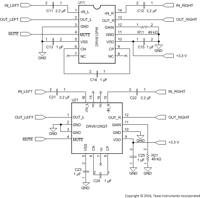
The DRV612 starts its operation by asserting the MUTE pin to logic 1. The device enters in mute mode when pulling low MUTE pin. The charge pump generates a negative supply voltage. The charge pump flying capacitor connected between CP and CN transfers charge to generate the negative supply voltage. The output voltages are capable of positive and negative voltage swings and are centered close to 0 V, eliminating the need for output capacitors. Input coupling capacitors block any dc bias from the audio source and ensure maximum dynamic range.
This typical connection diagram highlights the required external components and system level connections for proper operation of the device in popular use case. Any design variation can be supported by TI through schematic and layout reviews. Visit e2e.ti.com for design assistance and join the audio amplifier discussion forum for additional information.
10.1.1 Capacitive Load
The DRV612 has the ability to drive a high capacitive load up to 220 pF directly. Higher capacitive loads can be accepted by adding a series resistor of 47 Ω or larger for the line driver output.
10.2 Typical Application
 Figure 11. Single-Ended Input and Output, Gain Set to –1.5×
10.2.1 Design Requirements
Table 1 lists the design parameters for this application example.
Table 1. Typical Application Design Requirements
| PARAMETER | VALUE |
|---|---|
| Input voltage supply | 3 V to 3.6 V |
| Current | 130 mA |
| Load impedance | 32 Ω |
10.2.2 Detailed Design Procedure
10.2.2.1 Component Selection
10.2.2.1.1 Charge Pump Flying Capacitor and VSS Capacitor
The charge-pump flying capacitor serves to transfer charge during the generation of the negative supply voltage. The VSS capacitor must be at least equal to the charge pump capacitor in order to allow maximum charge transfer. Low-ESR capacitors are an ideal selection, and a value of 1 μF is typical.
10.2.2.1.2 Decoupling Capacitors
The DRV612 is a DirectPath line-driver amplifier that requires adequate power-supply decoupling to ensure that the noise and total harmonic distortion (THD) are low. A good low equivalent-series-resistance (ESR) ceramic capacitor, typically 1 μF, placed as close as possible to the device VDD lead works best. Placing this decoupling capacitor close to the DRV612 is important for the performance of the amplifier. For filtering lower-frequency noise signals, a 10-μF or greater capacitor placed near the audio power amplifier also helps, but it is not required in most applications because of the high PSRR of this device.
10.2.2.1.3 Gain-Setting
The gain setting is programmed with the GAIN pin. Gain setting is latched during power on. Table 2 lists the gain settings.
NOTE
If gain pin is left unconnected (open) default gain of –2× is selected.
Table 2. Gain Settings
10.2.2.1.4 Input-Blocking Capacitors
DC input-blocking capacitors are required to be added in series with the audio signal into the input pins of the DRV612. These capacitors block the dc portion of the audio source and allow the DRV612 inputs to be properly biased to provide maximum performance. The input blocking capacitors also limit the dc gain to 1, limiting the dc-offset voltage at the output.
These capacitors form a high-pass filter with the input resistor, RIN. The cutoff frequency is calculated using Equation 1. For this calculation, the capacitance used is the input-blocking capacitor and the resistance is the input resistor chosen from Table 3. Then the frequency and/or capacitance can be determined when one of the two values is given.

For a fixed cutoff frequency of 2 Hz, the size of the input capacitance is shown in Table 3 with the capacitors rounded up to nearest E6 values. For 20-Hz cutoff, simply divide the capacitor values with 10; for example, for 1× gain, 150 nF is needed.
Table 3. Input Capacitor for Different Gain and Cutoff
10.2.3 Application Curves
The characteristics of this design are shown in Table 4.
Table 4. Table of Graphs
| FIGURE | |
|---|---|
| THD+N vs Output Voltage 3.3 V, 10 kΩ, 1 kHz | Figure 1 |
| THD+N vs Output Voltage 3.3 V, 600-Ω Load, 1 kHz | Figure 2 |
| THD+N vs Frequency 3.3 V, 10-kΩ Load, 2 Vrms | Figure 3 |
| Channel Separation 3.3 V, 5-kΩ Load, 2 Vrms | Figure 4 |
| Gain vs Frequency for the Different Gain Settings | Figure 5 |
| Mute to Play | Figure 6 |
| Play to Mute | Figure 7 |