JAJSKK7 November   2021 DRV8231

PRODUCTION DATA  

  1. 特長
  2. アプリケーション
  3. 概要
  4. Revision History
  5. Device Comparison
  6. Pin Configuration and Functions
  7. Specifications
    1. 7.1 Absolute Maximum Ratings
    2. 7.2 ESD Ratings
    3. 7.3 Recommended Operating Conditions
    4. 7.4 Thermal Information
    5. 7.5 Electrical Characteristics
    6. 7.6 Typical Characteristics
    7. 7.7 Timing Diagrams
  8. Detailed Description
    1. 8.1 Overview
    2. 8.2 Functional Block Diagram
    3. 8.3 External Components
    4. 8.4 Feature Description
      1. 8.4.1 Bridge Control
      2. 8.4.2 Current Regulation
      3. 8.4.3 Protection Circuits
        1. 8.4.3.1 Overcurrent Protection (OCP)
        2. 8.4.3.2 Thermal Shutdown (TSD)
        3. 8.4.3.3 VM Undervoltage Lockout (UVLO)
    5. 8.5 Device Functional Modes
      1. 8.5.1 Active Mode
      2. 8.5.2 Low-Power Sleep Mode
      3. 8.5.3 Fault Mode
    6. 8.6 Pin Diagrams
      1. 8.6.1 Logic-Level Inputs
  9. Application and Implementation
    1. 9.1 Application Information
    2. 9.2 Typical Application
      1. 9.2.1 Brush DC Motor
        1. 9.2.1.1 Design Requirements
        2. 9.2.1.2 Detailed Design Procedure
          1. 9.2.1.2.1 Motor Voltage
          2. 9.2.1.2.2 Motor Current
          3. 9.2.1.2.3 Sense Resistor
        3. 9.2.1.3 Application Curves
      2. 9.2.2 Stall Detection
        1. 9.2.2.1 Design Requirements
        2. 9.2.2.2 Detailed Design Procedure
          1. 9.2.2.2.1 Stall Detection Timing
          2. 9.2.2.2.2 Stall Threshold Selection
        3. 9.2.2.3 Application Curves
      3. 9.2.3 Relay Driving
        1. 9.2.3.1 Design Requirements
        2. 9.2.3.2 Detailed Design Procedure
          1. 9.2.3.2.1 Control Interface for Single-Coil Relays
          2. 9.2.3.2.2 Control Interface for Dual-Coil Relays
        3. 9.2.3.3 Application Curves
      4. 9.2.4 Multi-Sourcing with Standard Motor Driver Pinout
    3. 9.3 Current Capability and Thermal Performance
      1. 9.3.1 Power Dissipation and Output Current Capability
      2. 9.3.2 Thermal Performance
        1. 9.3.2.1 Steady-State Thermal Performance
        2. 9.3.2.2 Transient Thermal Performance
  10. 10Power Supply Recommendations
    1. 10.1 Bulk Capacitance
  11. 11Layout
    1. 11.1 Layout Guidelines
    2. 11.2 Layout Example
  12. 12Device and Documentation Support
    1. 12.1 Documentation Support
      1. 12.1.1 Related Documentation
    2. 12.2 Receiving Notification of Documentation Updates
    3. 12.3 Community Resources
    4. 12.4 Trademarks
  13. 13Mechanical, Packaging, and Orderable Information

パッケージ・オプション

メカニカル・データ(パッケージ|ピン)
サーマルパッド・メカニカル・データ
発注情報

Current Regulation

The DRV8231 device limits the output current based on the analog input, VREF, and the resistance of an external sense resistor on the ISEN pin, RSENSE, according to Equation 1:

Equation 1. ITRIP=VREFAV×RSENSE=VREF10×RSENSE

By using current regulation, the device input pins can be set for 100% duty cycle, while the device switches the outputs to keep the motor current at the ITRIP level. For example, if VREF = 3.3 V and a RSENSE = 0.15 Ω, the DRV8231 limits motor current to 2.2 A during high torque conditions. For guidelines on selecting a sense resistor, see the Section 9.2.1.2.3 section.

When ITRIP is reached, the device enforces slow current decay by enabling both low-side FETs, and it does this for a time of tOFF.
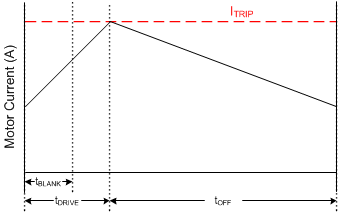
GUID-CDDE39F4-1CDA-4B27-9D32-E975FFB6137E-low.gif Figure 8-3 Current-Regulation Time Periods

After tOFF elapses, the output is re-enabled according to the two inputs, INx. The drive time (tDRIVE) until reaching another ITRIP event heavily depends on the VM voltage, the back-EMF of the motor, and the inductance of the motor.

If current regulation is not required, the ISEN pin should be directly connected to the PCB ground plane. The VREF voltage must still be 0.3 V to 5 V, and larger voltages provide greater noise margin. This provides the highest-possible peak current which is up to IOCP,min for a few hundred milliseconds (depending on PCB characteristics and the ambient temperature). If current exceeds IOCP,min, the device may enter the fault mode due to overcurrent protection (OCP) or overtemperature shutdown (TSD).