JAJSNH4 April   2022 DRV8300-Q1

PRODUCTION DATA  

  1. 特長
  2. アプリケーション
  3. 概要
  4. Revision History
  5. Device Comparison Table
  6. Pin Configuration and Functions
  7. Specifications
    1. 7.1 Absolute Maximum Ratings
    2. 7.2 ESD Ratings AUTO
    3. 7.3 Recommended Operating Conditions
    4. 7.4 Thermal Information
    5. 7.5 Electrical Characteristics
    6. 7.6 Timing Diagrams
    7. 7.7 Typical Characteristics
  8. Detailed Description
    1. 8.1 Overview
    2. 8.2 Functional Block Diagram
    3. 8.3 Feature Description
      1. 8.3.1 Three BLDC Gate Drivers
        1. 8.3.1.1 Gate Drive Timings
          1. 8.3.1.1.1 Propagation Delay
          2. 8.3.1.1.2 Deadtime and Cross-Conduction Prevention
        2. 8.3.1.2 Gate Driver Outputs
      2. 8.3.2 Pin Diagrams
      3. 8.3.3 Gate Driver Protective Circuits
        1. 8.3.3.1 VBSTx Undervoltage Lockout (BSTUV)
        2. 8.3.3.2 GVDD Undervoltage Lockout (GVDDUV)
    4. 8.4 Device Functional Modes
  9. Application and Implementation
    1. 9.1 Application Information
    2. 9.2 Typical Application
      1. 9.2.1 Design Requirements
      2. 9.2.2 Bootstrap Capacitor and GVDD Capacitor Selection
      3. 9.2.3 Application Curves
  10. 10Power Supply Recommendations
  11. 11Layout
    1. 11.1 Layout Guidelines
  12. 12Device and Documentation Support
    1. 12.1 Receiving Notification of Documentation Updates
    2. 12.2 サポート・リソース
    3. 12.3 Trademarks
    4. 12.4 Electrostatic Discharge Caution
    5. 12.5 Glossary
  13. 13Mechanical, Packaging, and Orderable Information

パッケージ・オプション

メカニカル・データ(パッケージ|ピン)
サーマルパッド・メカニカル・データ
発注情報

Application Curves

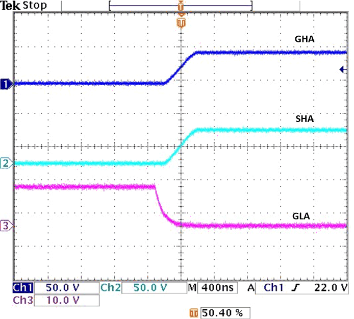
GUID-20201215-CA0I-VCZM-N0L2-LJWH9RDWCJCL-low.gifFigure 9-2 Gate voltages, SHx rising with 15 ohm gate resistor and CSD19532Q5B MOSFET
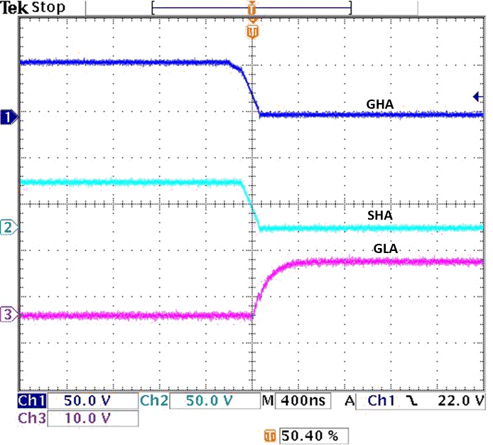
GUID-20201215-CA0I-T6T2-HQRB-XNCXKQXS2MFN-low.gifFigure 9-3 Gate voltages, SHx falling with 15 ohm gate resistor and CSD19532Q5B MOSFET