JAJSHP7D May   2015  – July 2019 DRV8305-Q1

PRODUCTION DATA.  

  1. 特長
  2. アプリケーション
  3. 概要
    1.     Device Images
      1.      概略回路図
  4. 改訂履歴
  5. 概要(続き)
  6. Pin Configuration and Functions
    1.     Pin Functions
  7. Specifications
    1. 7.1 Absolute Maximum Ratings
    2. 7.2 ESD Ratings
    3. 7.3 Recommended Operating Conditions
    4. 7.4 Thermal Information
    5. 7.5 Electrical Characteristics
    6. 7.6 SPI Timing Requirements (Slave Mode Only)
    7. 7.7 Typical Characteristics
  8. Detailed Description
    1. 8.1 Overview
    2. 8.2 Functional Block Diagram
    3. 8.3 Feature Description
      1. 8.3.1 Integrated Three-Phase Gate Driver
      2. 8.3.2 INHx/INLx: Gate Driver Input Modes
      3. 8.3.3 VCPH Charge Pump: High-Side Gate Supply
      4. 8.3.4 VCP_LSD LDO: Low-Side Gate Supply
      5. 8.3.5 GHx/GLx: Half-Bridge Gate Drivers
        1. 8.3.5.1 Smart Gate Drive Architecture: IDRIVE
        2. 8.3.5.2 Smart Gate Drive Architecture: TDRIVE
        3. 8.3.5.3 CSAs: Current Shunt Amplifiers
      6. 8.3.6 DVDD and AVDD: Internal Voltage Regulators
      7. 8.3.7 VREG: Voltage Regulator Output
      8. 8.3.8 Protection Features
        1. 8.3.8.1 Fault and Warning Classification
        2. 8.3.8.2 MOSFET Shoot-Through Protection (TDRIVE)
        3. 8.3.8.3 MOSFET Overcurrent Protection (VDS_OCP)
          1. 8.3.8.3.1 MOSFET dV/dt Turn On Protection (TDRIVE)
          2. 8.3.8.3.2 MOSFET Gate Drive Protection (GDF)
        4. 8.3.8.4 Low-Side Source Monitors (SNS_OCP)
        5. 8.3.8.5 Fault and Warning Operating Modes
      9. 8.3.9 Undervoltage Warning (UVFL), Undervoltage Lockout (UVLO), and Overvoltage (OV) Protection
        1. 8.3.9.1 Overtemperature Warning (OTW) and Shutdown (OTSD) Protection
        2. 8.3.9.2 Reverse Supply Protection
        3. 8.3.9.3 MCU Watchdog
        4. 8.3.9.4 VREG Undervoltage (VREG_UV)
        5. 8.3.9.5 Latched Fault Reset Methods
    4. 8.4 Device Functional Modes
      1. 8.4.1 Power Up Sequence
      2. 8.4.2 Standby State
      3. 8.4.3 Operating State
      4. 8.4.4 Sleep State
      5. 8.4.5 Limp Home or Fail Code Operation
    5. 8.5 Programming
      1. 8.5.1 SPI Communication
        1. 8.5.1.1 SPI
        2. 8.5.1.2 SPI Format
    6. 8.6 Register Maps
      1. 8.6.1 Status Registers
        1. 8.6.1.1 Warning and Watchdog Reset (Address = 0x1)
          1. Table 10. Warning and Watchdog Reset Register Description
        2. 8.6.1.2 OV/VDS Faults (Address = 0x2)
          1. Table 11. OV/VDS Faults Register Description
        3. 8.6.1.3 IC Faults (Address = 0x3)
          1. Table 12. IC Faults Register Description
        4. 8.6.1.4 VGS Faults (Address = 0x4)
          1. Table 13. Gate Driver VGS Faults Register Description
      2. 8.6.2 Control Registers
        1. 8.6.2.1 HS Gate Drive Control (Address = 0x5)
          1. Table 14. HS Gate Driver Control Register Description
        2. 8.6.2.2 LS Gate Drive Control (Address = 0x6)
          1. Table 15. LS Gate Driver Control Register Description
        3. 8.6.2.3 Gate Drive Control (Address = 0x7)
          1. Table 16. Gate Drive Control Register Description
        4. 8.6.2.4 IC Operation (Address = 0x9)
          1. Table 17. IC Operation Register Description
        5. 8.6.2.5 Shunt Amplifier Control (Address = 0xA)
          1. Table 18. Shunt Amplifier Control Register Description
        6. 8.6.2.6 Voltage Regulator Control (Address = 0xB)
          1. Table 19. Voltage Regulator Control Register Description
        7. 8.6.2.7 VDS Sense Control (Address = 0xC)
          1. Table 20. VDS Sense Control Register Description
  9. Application and Implementation
    1. 9.1 Application Information
    2. 9.2 Typical Application
      1. 9.2.1 Design Requirements
      2. 9.2.2 Detailed Design Procedure
        1. 9.2.2.1 Gate Drive Average Current
        2. 9.2.2.2 MOSFET Slew Rates
        3. 9.2.2.3 Overcurrent Protection
        4. 9.2.2.4 Current Sense Amplifiers
      3. 9.2.3 VREG Reference Voltage Input (DRV8305N)
      4. 9.2.4 Application Curves
  10. 10Power Supply Recommendations
    1. 10.1 Power Supply Consideration in Generator Mode
    2. 10.2 Bulk Capacitance
  11. 11Layout
    1. 11.1 Layout Guidelines
    2. 11.2 Layout Example
  12. 12デバイスおよびドキュメントのサポート
    1. 12.1 ドキュメントのサポート
    2. 12.2 ドキュメントの更新通知を受け取る方法
    3. 12.3 コミュニティ・リソース
    4. 12.4 商標
    5. 12.5 静電気放電に関する注意事項
    6. 12.6 Glossary
  13. 13メカニカル、パッケージ、および注文情報

パッケージ・オプション

メカニカル・データ(パッケージ|ピン)
サーマルパッド・メカニカル・データ
発注情報

Bulk Capacitance

Having appropriate local bulk capacitance is an important factor in motor drive system design. It is generally beneficial to have more bulk capacitance, while the disadvantages are increased cost and physical size.

The amount of local capacitance needed depends on a variety of factors, including the:

  • Highest current required by the motor system
  • Power supply’s capacitance and ability to source or sink current
  • Amount of parasitic inductance between the power supply and motor system
  • Acceptable voltage ripple
  • Type of motor used (brushed DC, brushless DC, stepper)
  • Motor braking method

The inductance between the power supply and motor drive system will limit the rate that current can change from the power supply. If the local bulk capacitance is too small, the system will respond to excessive current demands or dumps from the motor with a change in voltage. When adequate bulk capacitance is used, the motor voltage remains stable and high current can be quickly supplied.

The data sheet generally provides a recommended value, but system-level testing is required to determine the appropriate-sized bulk capacitor.
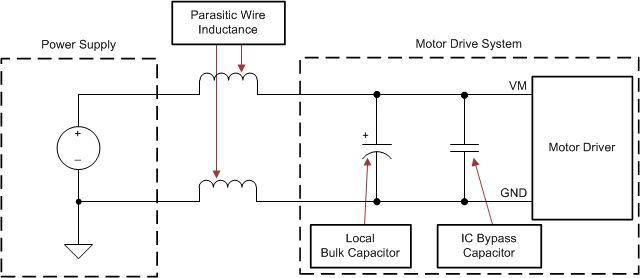
DRV8305-Q1 mtr_drv_sys_lvscx2.gifFigure 25. Example Setup of Motor Drive System With External Power Supply

The voltage rating for bulk capacitors should be higher than the operating voltage, to provide margin for cases when the motor transfers energy to the supply.