JAJSF51A April   2018  – July 2018 DRV8306

PRODUCTION DATA.  

  1. 特長
  2. アプリケーション
  3. 概要
    1.     概略回路図
  4. 改訂履歴
  5. 概要(続き)
  6. Pin Configuration and Functions
    1.     Pin Functions
  7. Specifications
    1. 7.1 Absolute Maximum Ratings
    2. 7.2 ESD Ratings
    3. 7.3 Recommended Operating Conditions
    4. 7.4 Thermal Information
    5. 7.5 Electrical Characteristics
    6. 7.6 Typical Characteristics
  8. Detailed Description
    1. 8.1 Overview
    2. 8.2 Functional Block Diagram
    3. 8.3 Feature Description
      1. 8.3.1 Three Phase Smart Gate Drivers
        1. 8.3.1.1 PWM Control Mode (1x PWM Mode)
        2. 8.3.1.2 Hardware Interface Mode
        3. 8.3.1.3 Gate Driver Voltage Supplies
        4. 8.3.1.4 Smart Gate Drive Architecture
          1. 8.3.1.4.1 IDRIVE: MOSFET Slew-Rate Control
          2. 8.3.1.4.2 TDRIVE: MOSFET Gate Drive Control
          3. 8.3.1.4.3 Gate Drive Clamp
          4. 8.3.1.4.4 Propagation Delay
          5. 8.3.1.4.5 MOSFET VDS Monitors
          6. 8.3.1.4.6 VDRAIN Sense Pin
      2. 8.3.2 DVDD Linear Voltage Regulator
      3. 8.3.3 Pulse-by-Pulse Current Limit
      4. 8.3.4 Hall Comparators
      5. 8.3.5 FGOUT Signal
      6. 8.3.6 Pin Diagrams
      7. 8.3.7 Gate-Driver Protective Circuits
        1. 8.3.7.1 VM Supply Undervoltage Lockout (UVLO)
        2. 8.3.7.2 VCP Charge-Pump Undervoltage Lockout (CPUV)
        3. 8.3.7.3 MOSFET VDS Overcurrent Protection (VDS_OCP)
        4. 8.3.7.4 VSENSE Overcurrent Protection (SEN_OCP)
        5. 8.3.7.5 Gate Driver Fault (GDF)
        6. 8.3.7.6 Thermal Shutdown (OTSD)
    4. 8.4 Device Functional Modes
      1. 8.4.1 Gate Driver Functional Modes
        1. 8.4.1.1 Sleep Mode
        2. 8.4.1.2 Operating Mode
        3. 8.4.1.3 Fault Reset (ENABLE Reset Pulse)
  9. Application and Implementation
    1. 9.1 Application Information
      1. 9.1.1 Hall Sensor Configuration and Connection
        1. 9.1.1.1 Typical Configuration
        2. 9.1.1.2 Open Drain Configuration
        3. 9.1.1.3 Series Configuration
        4. 9.1.1.4 Parallel Configuration
    2. 9.2 Typical Application
      1. 9.2.1 Primary Application
        1. 9.2.1.1 Design Requirements
        2. 9.2.1.2 Detailed Design Procedure
          1. 9.2.1.2.1 External MOSFET Support
            1. 9.2.1.2.1.1 Example
          2. 9.2.1.2.2 IDRIVE Configuration
            1. 9.2.1.2.2.1 Example
          3. 9.2.1.2.3 VDS Overcurrent Monitor Configuration
            1. 9.2.1.2.3.1 Example
        3. 9.2.1.3 Application Curves
  10. 10Power Supply Recommendations
    1. 10.1 Bulk Capacitance Sizing
  11. 11Layout
    1. 11.1 Layout Guidelines
    2. 11.2 Layout Example
  12. 12デバイスおよびドキュメントのサポート
    1. 12.1 デバイス・サポート
      1. 12.1.1 デバイスの項目表記
    2. 12.2 ドキュメントのサポート
      1. 12.2.1 関連資料
    3. 12.3 ドキュメントの更新通知を受け取る方法
    4. 12.4 コミュニティ・リソース
    5. 12.5 商標
    6. 12.6 静電気放電に関する注意事項
    7. 12.7 Glossary
  13. 13メカニカル、パッケージ、および注文情報

パッケージ・オプション

メカニカル・データ(パッケージ|ピン)
サーマルパッド・メカニカル・データ
発注情報

Gate Driver Voltage Supplies

The high-side gate-drive voltage supply is created using a doubler charge pump that operates from the VM voltage supply input. The charge pump lets the gate driver correctly bias the high-side MOSFET gate with respect to its source across a wide input supply voltage range. The charge pump is regulated to maintain a fixed output voltage of VVM + 10 V and supports an average output current of 15 mA. When the VVM voltage is less than 12 V, the charge pump operates in full doubler mode and generates VVCP = 2 × VVM – 1.5 V when unloaded. The charge pump is continuously monitored for undervoltage to prevent under-driven MOSFET conditions. The charge pump requires a X5R or X7R, 1-µF, 16-V ceramic capacitor between the VM and VCP pins to act as the storage capacitor. Additionally, a X5R or X7R, 22-nF, VM-rated ceramic capacitor is required between the CPH and CPL pins to act as the flying capacitor.
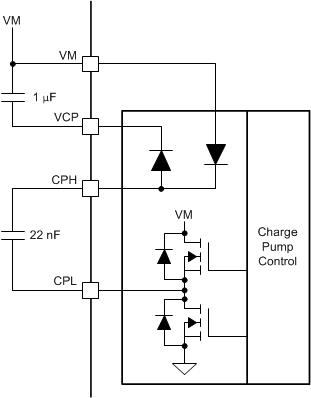
DRV8306 drv8306-charge-pump-architecture.gifFigure 11. Charge Pump Architecture

The low-side gate drive voltage is created using a linear low-dropout (LDO) regulator that operates from the VM voltage supply input. The LDO regulator allows the gate driver to properly bias the low-side MOSFET gate with respect to ground. The LDO regulator output is fixed at 10 V and supports an output current of 15 mA. The LDO regulator is monitored for undervoltage to prevent under-driven MOSFET conditions.