JAJSMZ5B September   2021  – February 2022 DRV8311

PRODUCTION DATA  

  1. 特長
  2. アプリケーション
  3. 概要
  4. Revision History
  5. Device Comparison Table
  6. Pin Configuration and Functions
  7. Specifications
    1. 7.1 Absolute Maximum Ratings
    2. 7.2 ESD Ratings
    3. 7.3 Recommended Operating Conditions
    4. 7.4 Thermal Information
    5. 7.5 Electrical Characteristics
    6. 7.6 SPI Timing Requirements
    7. 7.7 SPI Secondary Device Mode Timings
    8. 7.8 Typical Characteristics
  8. Detailed Description
    1. 8.1 Overview
    2. 8.2 Functional Block Diagram
    3. 8.3 Feature Description
      1. 8.3.1  Output Stage
      2. 8.3.2  Control Modes
        1. 8.3.2.1 6x PWM Mode (DRV8311S and DRV8311H variants only)
        2. 8.3.2.2 3x PWM Mode (DRV8311S and DRV8311H variants only)
        3. 8.3.2.3 PWM Generation Mode (DRV8311S and DRV8311P Variants)
      3. 8.3.3  Device Interface Modes
        1. 8.3.3.1 Serial Peripheral Interface (SPI)
        2. 8.3.3.2 Hardware Interface
      4. 8.3.4  AVDD Linear Voltage Regulator
      5. 8.3.5  Charge Pump
      6. 8.3.6  Slew Rate Control
      7. 8.3.7  Cross Conduction (Dead Time)
      8. 8.3.8  Propagation Delay
      9. 8.3.9  Pin Diagrams
        1. 8.3.9.1 Logic Level Input Pin (Internal Pulldown)
        2. 8.3.9.2 Logic Level Input Pin (Internal Pullup)
        3. 8.3.9.3 Open Drain Pin
        4. 8.3.9.4 Push Pull Pin
        5. 8.3.9.5 Four Level Input Pin
      10. 8.3.10 Current Sense Amplifiers
        1. 8.3.10.1 Current Sense Amplifier Operation
        2. 8.3.10.2 Current Sense Amplifier Offset Correction
      11. 8.3.11 Protections
        1. 8.3.11.1 VM Supply Undervoltage Lockout (NPOR)
        2. 8.3.11.2 Under Voltage Protections (UVP)
        3. 8.3.11.3 Overcurrent Protection (OCP)
          1. 8.3.11.3.1 OCP Latched Shutdown (OCP_MODE = 010b)
          2. 8.3.11.3.2 OCP Automatic Retry (OCP_MODE = 000b or 001b)
          3. 8.3.11.3.3 OCP Report Only (OCP_MODE = 011b)
          4. 8.3.11.3.4 OCP Disabled (OCP_MODE = 111b)
        4. 8.3.11.4 Thermal Protections
          1. 8.3.11.4.1 Thermal Warning (OTW)
          2. 8.3.11.4.2 Thermal Shutdown (OTSD)
    4. 8.4 Device Functional Modes
      1. 8.4.1 Functional Modes
        1. 8.4.1.1 Sleep Mode
        2. 8.4.1.2 Operating Mode
        3. 8.4.1.3 Fault Reset (CLR_FLT or nSLEEP Reset Pulse)
    5. 8.5 SPI Communication
      1. 8.5.1 Programming
        1. 8.5.1.1 SPI and tSPI Format
  9. DRV8311 Registers
  10. 10Application and Implementation
    1. 10.1 Application Information
    2. 10.2 Typical Applications
      1. 10.2.1 Three-Phase Brushless-DC Motor Control
        1. 10.2.1.1 Detailed Design Procedure
          1. 10.2.1.1.1 Motor Voltage
        2. 10.2.1.2 Driver Propagation Delay and Dead Time
        3. 10.2.1.3 Delay Compensation
        4. 10.2.1.4 Current Sensing and Output Filtering
        5. 10.2.1.5 Application Curves
    3. 10.3 Three Phase Brushless-DC tSPI Motor Control
      1. 10.3.1 Detailed Design Procedure
    4. 10.4 Alternate Applications
  11. 11Power Supply Recommendations
    1. 11.1 Bulk Capacitance
  12. 12Layout
    1. 12.1 Layout Guidelines
    2. 12.2 Layout Example
    3. 12.3 Thermal Considerations
      1. 12.3.1 Power Dissipation and Junction Temperature Estimation
  13. 13Device and Documentation Support
    1. 13.1 サポート・リソース
    2. 13.2 Trademarks
    3. 13.3 Electrostatic Discharge Caution
    4. 13.4 Glossary
  14. 14Mechanical, Packaging, and Orderable Information

パッケージ・オプション

メカニカル・データ(パッケージ|ピン)
サーマルパッド・メカニカル・データ
発注情報

Current Sense Amplifier Operation

The SOx pin on the DRV8311 outputs an analog voltage proportional to current flowing in the low side FETs (IOUTx) multiplied by the gain setting (GCSA). The gain setting is adjustable between four different levels which can be set by the GAIN pin (hardware device variant) or the CSA_GAIN bits (SPI or tSPI device variant).

Figure 8-28 shows the internal architecture of the current sense amplifiers. The current sense is implemented with a sense FET on each low-side FET of the DRV8311 device. This current information is converted in to a voltage, which generates the CSA output voltage on the SOx pin, based on the voltage on the CSAREF pin (VREF) and the gain setting. The CSA output voltage can be calculated using Equation 15

Equation 2. SOx= VREF2±(GCSA×IOUTx)
Figure 8-28 Integrated Current Sense Amplifier

Figure 8-29 and Figure 8-30 show the details of the amplifier operational range. In bi-directional operation, the amplifier output for 0-V input is set at VREF/2. Any change in the differential input results in a corresponding change in the output times the GCSA factor. The amplifier has a defined linear region in which it can maintain operation.
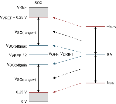
GUID-88606CB7-5356-4277-9D88-7340882F761F-low.gifFigure 8-29 Bidirectional Current Sense Output
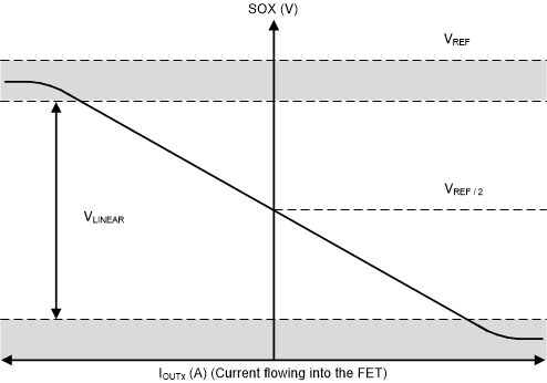
GUID-22BC5078-92B9-47D6-A8AD-6365C0DBDF1C-low.gifFigure 8-30 Bidirectional Current Sense Regions
Note: The current sense amplifiers uses the external voltage reference (VREF) provided at the CSAREF pin.