JAJSMZ5B September 2021 – February 2022 DRV8311
PRODUCTION DATA
- 1 特長
- 2 アプリケーション
- 3 概要
- 4 Revision History
- 5 Device Comparison Table
- 6 Pin Configuration and Functions
- 7 Specifications
-
8 Detailed Description
- 8.1 Overview
- 8.2 Functional Block Diagram
- 8.3
Feature Description
- 8.3.1 Output Stage
- 8.3.2 Control Modes
- 8.3.3 Device Interface Modes
- 8.3.4 AVDD Linear Voltage Regulator
- 8.3.5 Charge Pump
- 8.3.6 Slew Rate Control
- 8.3.7 Cross Conduction (Dead Time)
- 8.3.8 Propagation Delay
- 8.3.9 Pin Diagrams
- 8.3.10 Current Sense Amplifiers
- 8.3.11 Protections
- 8.4 Device Functional Modes
- 8.5 SPI Communication
- 9 DRV8311 Registers
- 10Application and Implementation
- 11Power Supply Recommendations
- 12Layout
- 13Device and Documentation Support
- 14Mechanical, Packaging, and Orderable Information
8.3.9.2 Logic Level Input Pin (Internal Pullup)
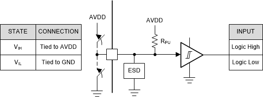
Figure 8-24 shows the input structure for the logic level pin nSCS. The input can be driven with an external resistor to GND or an external logic voltage supply .
 Figure 8-24 nSCS Input Pin Structure