JAJSHI4 May 2019 DRV8340-Q1
PRODUCTION DATA.
- 1 特長
- 2 アプリケーション
- 3 概要
- 4 改訂履歴
- 5 Device Comparison Table
- 6 Pin Configuration and Functions
- 7 Specifications
-
8 Detailed Description
- 8.1 Overview
- 8.2 Functional Block Diagram
- 8.3
Feature Description
- 8.3.1
Three Phase Smart Gate Drivers
- 8.3.1.1
PWM Control Modes
- 8.3.1.1.1 6x PWM Mode (PWM_MODE = 000b or MODE Pin Tied to AGND)
- 8.3.1.1.2 3x PWM Mode (PWM_MODE = 001b or MODE Pin = 18 kΩ to AGND)
- 8.3.1.1.3 1x PWM Mode (PWM_MODE = 010b or MODE Pin = 75 kΩ to AGND)
- 8.3.1.1.4 Independent Half-Bridge PWM Mode (PWM_MODE = 011b or MODE Pin is > 1.5 MΩ to AGND or Hi-Z)
- 8.3.1.1.5 Phases A and B are Independent Half-Bridges, Phase C is Independent FET (MODE = 100b)
- 8.3.1.1.6 Phases B and C are Independent Half-Bridges, Phase A is Independent FET (MODE = 101b or MODE Pin is 75 kΩ to DVDD)
- 8.3.1.1.7 Phases A is Independent Half-Bridge, Phases B and C are Independent FET (MODE = 110b or MODE Pin is 18 kΩ to DVDD)
- 8.3.1.1.8 Independent MOSFET Drive Mode (PWM_MODE = 111b or MODE Pin = 0.47 kΩ to DVDD)
- 8.3.1.2 Device Interface Modes
- 8.3.1.3 Gate Driver Voltage Supplies
- 8.3.1.4 Smart Gate Drive Architecture
- 8.3.1.1
PWM Control Modes
- 8.3.2 DVDD Linear Voltage Regulator
- 8.3.3 Pin Diagrams
- 8.3.4
Gate Driver Protective Circuits
- 8.3.4.1 VM Supply Undervoltage Lockout (UVLO)
- 8.3.4.2 VCP Charge Pump Undervoltage Lockout (CPUV)
- 8.3.4.3 MOSFET VDS Overcurrent Protection (VDS_OCP)
- 8.3.4.4 Gate Driver Fault (GDF)
- 8.3.4.5 Thermal Warning (OTW)
- 8.3.4.6 Thermal Shutdown (OTSD)
- 8.3.4.7 Open Load Detection (OLD)
- 8.3.4.8 Offline Shorts Diagnostics
- 8.3.4.9 Reverse Supply Protection
- 8.3.1
Three Phase Smart Gate Drivers
- 8.4 Device Functional Modes
- 8.5 Programming
- 8.6
Register Maps
- 8.6.1 Status Registers
- 8.6.2
Control Registers
- 8.6.2.1 IC1 Control Register (Address = 0x04) [reset = 0x00]
- 8.6.2.2 IC2 Control Register (address = 0x05) [reset = 0x40]
- 8.6.2.3 IC3 Control Register (Address = 0x06) [reset = 0xFF]
- 8.6.2.4 IC4 Control Register (Address = 0x07) [reset = 0xFF]
- 8.6.2.5 IC5 Control Register (Address = 0x08) [reset = 0xFF]
- 8.6.2.6 IC6 Control Register (Address = 0x09) [reset = 0x99]
- 8.6.2.7 IC7 Control Register (Address = 0x0A) [reset = 0x99]
- 8.6.2.8 IC8 Control Register (Address = 0x0B) [reset = 0x99]
- 8.6.2.9 IC9 Control Register (Address = 0x0C) [reset = 0x2F]
- 8.6.2.10 IC10 Control Register (Address = 0x0D) [reset = 0x61]
- 8.6.2.11 IC11 Control Register (Address = 0x0E) [reset = 0x00]
- 8.6.2.12 IC12 Control Register (Address = 0x0F) [reset = 0x2A]
- 8.6.2.13 IC13 Control Register (Address = 0x10) [reset = 0x7F]
- 8.6.2.14 IC14 Control Register (Address = 0x10) [reset = 0x00]
- 9 Application and Implementation
- 10Power Supply Recommendations
- 11Layout
- 12デバイスおよびドキュメントのサポート
- 13メカニカル、パッケージ、および注文情報
パッケージ・オプション
メカニカル・データ(パッケージ|ピン)
- PHP|48
サーマルパッド・メカニカル・データ
- PHP|48
発注情報
8.3.1.1.3 1x PWM Mode (PWM_MODE = 010b or MODE Pin = 75 kΩ to AGND)
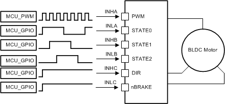
In 1x PWM mode, the DRV8340-Q1 device uses 6-step block commutation tables that are stored internally. This feature allows for a three-phase BLDC motor to be controlled using one PWM sourced from a simple controller. The PWM is applied on the INHA pin and determines the output frequency and duty cycle of the half-bridges.
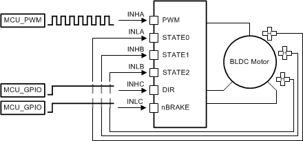
The half-bridge output states are managed by the INLA, INHB, and INLB pins which are used as state logic inputs. The state inputs can be controlled by an external controller or connected directly to the digital outputs of the Hall effect sensor from the motor (INLA = HALL_A, INHB = HALL_B, INLB = HALL_C). The 1x PWM mode usually operates with synchronous rectification (low-side MOSFET recirculation); however, the mode can be configured to use asynchronous rectification (MOSFET body diode freewheeling) on SPI devices. This configuration is set using the 1PWM_COM bit in the SPI registers.
The INHC input controls the direction through the 6-step commutation table which is used to change the direction of the motor when Hall effect sensors are directly controlling the state of the INLA, INHB, and INLB inputs. Tie the INHC pin low if this feature is not required.
The INLC input brakes the motor by turning off all high-side MOSFETs and turning on all low-side MOSFETs when the INLC pin is pulled low. This brake is independent of the state of the other input pins. Tie the INLC pin high if this feature is not required. In the SPI device, the brake and coast mode can also be selected by the 1PWM_BRAKE register (see Table 22).
Table 6. Synchronous 1x PWM Mode
| LOGIC AND HALL INPUTS | GATE DRIVE OUTPUTS(1) | ||||||||||||
|---|---|---|---|---|---|---|---|---|---|---|---|---|---|
| STATE | INHC = 0 | INHC = 1 | PHASE A | PHASE B | PHASE C | DESCRIPTION | |||||||
| INLA | INHB | INLB | INLA | INHB | INLB | GHA | GLA | GHB | GLB | GHC | GLC | ||
| Stop | 0 | 0 | 0 | 0 | 0 | 0 | L | L | L | L | L | L | Stop |
| Align | 1 | 1 | 1 | 1 | 1 | 1 | PWM | !PWM | L | H | L | H | Align |
| 1 | 1 | 1 | 0 | 0 | 0 | 1 | L | L | PWM | !PWM | L | H | B → C |
| 2 | 1 | 0 | 0 | 0 | 1 | 1 | PWM | !PWM | L | L | L | H | A → C |
| 3 | 1 | 0 | 1 | 0 | 1 | 0 | PWM | !PWM | L | H | L | L | A → B |
| 4 | 0 | 0 | 1 | 1 | 1 | 0 | L | L | L | H | PWM | !PWM | C → B |
| 5 | 0 | 1 | 1 | 1 | 0 | 0 | L | H | L | L | PWM | !PWM | C → A |
| 6 | 0 | 1 | 0 | 1 | 0 | 1 | L | H | PWM | !PWM | L | L | B → A |
Table 7. Asynchronous 1x PWM Mode 1PWM_COM = 1 (SPI Only)
| LOGIC AND HALL INPUTS | GATE DRIVE OUTPUTS | ||||||||||||
|---|---|---|---|---|---|---|---|---|---|---|---|---|---|
| STATE | INHC = 0 | INHC = 1 | PHASE A | PHASE B | PHASE C | DESCRIPTION | |||||||
| INLA | INHB | INLB | INLA | INHB | INLB | GHA | GLA | GHB | GLB | GHC | GLC | ||
| Stop | 0 | 0 | 0 | 0 | 0 | 0 | L | L | L | L | L | L | Stop |
| Align | 1 | 1 | 1 | 1 | 1 | 1 | PWM | L | L | H | L | H | Align |
| 1 | 1 | 1 | 0 | 0 | 0 | 1 | L | L | PWM | L | L | H | B → C |
| 2 | 1 | 0 | 0 | 0 | 1 | 1 | PWM | L | L | L | L | H | A → C |
| 3 | 1 | 0 | 1 | 0 | 1 | 0 | PWM | L | L | H | L | L | A → B |
| 4 | 0 | 0 | 1 | 1 | 1 | 0 | L | L | L | H | PWM | L | C → B |
| 5 | 0 | 1 | 1 | 1 | 0 | 0 | L | H | L | L | PWM | L | C → A |
| 6 | 0 | 1 | 0 | 1 | 0 | 1 | L | H | PWM | L | L | L | B → A |
Figure 10 and Figure 11 show the different possible configurations in 1x PWM mode.
 Figure 10. 1x PWM—Simple Controller
  Figure 11. 1x PWM—Hall Effect Sensor