JAJSHI4 May 2019 DRV8340-Q1
PRODUCTION DATA.
- 1 特長
- 2 アプリケーション
- 3 概要
- 4 改訂履歴
- 5 Device Comparison Table
- 6 Pin Configuration and Functions
- 7 Specifications
-
8 Detailed Description
- 8.1 Overview
- 8.2 Functional Block Diagram
- 8.3
Feature Description
- 8.3.1
Three Phase Smart Gate Drivers
- 8.3.1.1
PWM Control Modes
- 8.3.1.1.1 6x PWM Mode (PWM_MODE = 000b or MODE Pin Tied to AGND)
- 8.3.1.1.2 3x PWM Mode (PWM_MODE = 001b or MODE Pin = 18 kΩ to AGND)
- 8.3.1.1.3 1x PWM Mode (PWM_MODE = 010b or MODE Pin = 75 kΩ to AGND)
- 8.3.1.1.4 Independent Half-Bridge PWM Mode (PWM_MODE = 011b or MODE Pin is > 1.5 MΩ to AGND or Hi-Z)
- 8.3.1.1.5 Phases A and B are Independent Half-Bridges, Phase C is Independent FET (MODE = 100b)
- 8.3.1.1.6 Phases B and C are Independent Half-Bridges, Phase A is Independent FET (MODE = 101b or MODE Pin is 75 kΩ to DVDD)
- 8.3.1.1.7 Phases A is Independent Half-Bridge, Phases B and C are Independent FET (MODE = 110b or MODE Pin is 18 kΩ to DVDD)
- 8.3.1.1.8 Independent MOSFET Drive Mode (PWM_MODE = 111b or MODE Pin = 0.47 kΩ to DVDD)
- 8.3.1.2 Device Interface Modes
- 8.3.1.3 Gate Driver Voltage Supplies
- 8.3.1.4 Smart Gate Drive Architecture
- 8.3.1.1
PWM Control Modes
- 8.3.2 DVDD Linear Voltage Regulator
- 8.3.3 Pin Diagrams
- 8.3.4
Gate Driver Protective Circuits
- 8.3.4.1 VM Supply Undervoltage Lockout (UVLO)
- 8.3.4.2 VCP Charge Pump Undervoltage Lockout (CPUV)
- 8.3.4.3 MOSFET VDS Overcurrent Protection (VDS_OCP)
- 8.3.4.4 Gate Driver Fault (GDF)
- 8.3.4.5 Thermal Warning (OTW)
- 8.3.4.6 Thermal Shutdown (OTSD)
- 8.3.4.7 Open Load Detection (OLD)
- 8.3.4.8 Offline Shorts Diagnostics
- 8.3.4.9 Reverse Supply Protection
- 8.3.1
Three Phase Smart Gate Drivers
- 8.4 Device Functional Modes
- 8.5 Programming
- 8.6
Register Maps
- 8.6.1 Status Registers
- 8.6.2
Control Registers
- 8.6.2.1 IC1 Control Register (Address = 0x04) [reset = 0x00]
- 8.6.2.2 IC2 Control Register (address = 0x05) [reset = 0x40]
- 8.6.2.3 IC3 Control Register (Address = 0x06) [reset = 0xFF]
- 8.6.2.4 IC4 Control Register (Address = 0x07) [reset = 0xFF]
- 8.6.2.5 IC5 Control Register (Address = 0x08) [reset = 0xFF]
- 8.6.2.6 IC6 Control Register (Address = 0x09) [reset = 0x99]
- 8.6.2.7 IC7 Control Register (Address = 0x0A) [reset = 0x99]
- 8.6.2.8 IC8 Control Register (Address = 0x0B) [reset = 0x99]
- 8.6.2.9 IC9 Control Register (Address = 0x0C) [reset = 0x2F]
- 8.6.2.10 IC10 Control Register (Address = 0x0D) [reset = 0x61]
- 8.6.2.11 IC11 Control Register (Address = 0x0E) [reset = 0x00]
- 8.6.2.12 IC12 Control Register (Address = 0x0F) [reset = 0x2A]
- 8.6.2.13 IC13 Control Register (Address = 0x10) [reset = 0x7F]
- 8.6.2.14 IC14 Control Register (Address = 0x10) [reset = 0x00]
- 9 Application and Implementation
- 10Power Supply Recommendations
- 11Layout
- 12デバイスおよびドキュメントのサポート
- 13メカニカル、パッケージ、および注文情報
パッケージ・オプション
メカニカル・データ(パッケージ|ピン)
- PHP|48
サーマルパッド・メカニカル・データ
- PHP|48
発注情報
8.3.1.4.2 TDRIVE: MOSFET Gate Drive Control
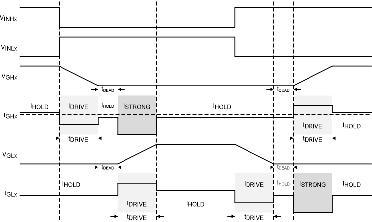
The TDRIVE component is an integrated gate drive state machine that provides automatic dead time insertion through handshaking between the high-side and low-side gate drivers, parasitic dV/dt gate turnon prevention, and MOSFET gate fault detection.
The first component of the TDRIVE state machine is automatic dead time insertion. Dead time is period of time between the switching of the external high-side and low-side MOSFETs to make sure that they do not cross conduct and cause shoot-through. The DRV8340-Q1 device uses VGS voltage monitors to measure the MOSFET gate-to-source voltage and determine the correct time to switch instead of relying on a fixed time value. This feature lets the dead time of the gate driver adjust for variation in the system such as temperature drift and variation in the MOSFET parameters. An additional digital dead time (tDEAD) can be inserted and is adjustable through the registers on SPI devices.
The second component of the TDRIVE state machine is parasitic dV/dt gate turnon prevention. To implement this component, the TDRIVE state machine enables a strong pulldown current (ISTRONG) on the opposite MOSFET gate whenever a MOSFET is switching. The strong pulldown occurs for the TDRIVE duration. This feature helps remove parasitic charge that couples into the MOSFET gate when the voltage half-bridge switch node slews rapidly.
The third component implements a gate-fault detection scheme to detect pin-to-pin solder defects, a MOSFET gate failure, or a MOSFET gate stuck-high or stuck-low voltage condition. This implementation is done with a pair of VGS gate-to-source voltage monitors for each half-bridge gate driver. When the gate driver receives a command to change the state of the half-bridge it starts to monitor the gate voltage of the external MOSFET. If, at the end of the tDRIVE period, the VGS voltage has not increased the correct threshold, the gate driver reports a fault. To make sure that a false gate drive fault (GDF) is not detected, a tDRIVE time should be selected that is longer than the time required to charge or discharge the MOSFET gate. The tDRIVE time does not increase the PWM time and will terminate if another PWM command is received while active. In the SPI device, for IDRIVE bit settings of 0000b, 0001b, 0010b, and 0011b, a longer tDRIVE time of 20-µs is automatically selected by the TDRIVE_MAX bit. If the 20-µs tDRVIE time is not required, write a 0 to the TDRIVE_MAX bit to disable it and set the tDRIVE time by the TDRIVE bits. For all other IDRIVE settings, writing to the TDRIVE_MAX bit is disabled. This option is not available in the H/W device.
For additional details on the TDRIVE settings, see the Register Maps section for SPI devices and the Pin Diagrams section for hardware interface devices. Figure 21 shows an example of the TDRIVE state machine in operation.
 Figure 21. TDRIVE State Machine