JAJSPA5 July 2020 DRV8353M
PRODUCTION DATA
- 1 特長
- 2 アプリケーション
- 3 概要
- 4 Revision History
- 5 Device Comparison Table
- 6 Pin Configuration and Functions
- 7 Absolute Maximum Ratings
- 8 ESD Ratings
- 9 Recommended Operating Conditions
- 10Thermal Information
- 11Electrical Characteristics
- 12SPI Timing Requirements
-
13Detailed Description
- 13.1 Overview
- 13.2 Functional Block Diagram
- 13.3
Feature Description
- 13.3.1 Three Phase Smart Gate Drivers
- 13.3.2 DVDD Linear Voltage Regulator
- 13.3.3 Pin Diagrams
- 13.3.4 Low-Side Current-Shunt Amplifiers
- 13.3.5
Gate Driver Protective Circuits
- 13.3.5.1 VM Supply and VDRAIN Undervoltage Lockout (UVLO)
- 13.3.5.2 VCP Charge-Pump and VGLS Regulator Undervoltage Lockout (GDUV)
- 13.3.5.3 MOSFET VDS Overcurrent Protection (VDS_OCP)
- 13.3.5.4 VSENSE Overcurrent Protection (SEN_OCP)
- 13.3.5.5 Gate Driver Fault (GDF)
- 13.3.5.6 Overcurrent Soft Shutdown (OCP Soft)
- 13.3.5.7 Thermal Warning (OTW)
- 13.3.5.8 Thermal Shutdown (OTSD)
- 13.3.5.9 Fault Response Table
- 13.4 Device Functional Modes
- 13.5 Programming
- 13.6
Register Maps
- 13.6.1 Status Registers
- 13.6.2
Control Registers
- 13.6.2.1 Driver Control Register (address = 0x02h)
- 13.6.2.2 Gate Drive HS Register (address = 0x03h)
- 13.6.2.3 Gate Drive LS Register (address = 0x04h)
- 13.6.2.4 OCP Control Register (address = 0x05h)
- 13.6.2.5 CSA Control Register (address = 0x06h)
- 13.6.2.6 Driver Configuration Register (address = 0x07h)
-
14Application and Implementation
- 14.1 Application Information
- 14.2
Typical Application
- 14.2.1
Primary Application
- 14.2.1.1 Design Requirements
- 14.2.1.2 Detailed Design Procedure
- 14.2.1.3 Application Curves
- 14.2.1
Primary Application
- 15Power Supply Recommendations
- 16Layout
- 17Device and Documentation Support
- 18Mechanical, Packaging, and Orderable Information
13.3.1.3 Gate Driver Voltage Supplies and Input Supply Configurations
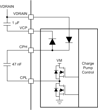
The high-side gate-drive voltage supply is created using a doubler charge pump that operates from the VM and VDRAIN voltage supply inputs. The charge pump allows the gate driver to correctly bias the high-side MOSFET gate with respect to the source across a wide input supply voltage range. The charge pump is regulated to keep a fixed output voltage of VVDRAIN + 10.5 V and supports an average output current of 25 mA. When VVM is less than 12 V, the charge pump operates in full doubler mode and generates VVCP = 2 × VVM – 1.5 V with respect to VVDRAIN when unloaded. The charge pump is continuously monitored for undervoltage to prevent under-driven MOSFET conditions.
The charge pump requires a X5R or X7R, 1-µF, 16-V ceramic capacitor between the VDRAIN and VCP pins to act as the storage capacitor. Additionally, a X5R or X7R, 47-nF, VDRAIN-rated ceramic capacitor is required between the CPH and CPL pins to act as the flying capacitor.
 Figure 13-10 Charge Pump Architecture
The low-side gate drive voltage is created using a linear regulator that operates from the VM voltage supply input. The VGLS linear regulator allows the gate driver to correctly bias the low-side MOSFET gate with respect to ground. The VGLS linear regulator output is fixed at 14.5 V and further regulated to 11-V on the GLx outputs during operation. The VGLS regulator supports an output current of 25 mA. The VGLS linear regulator is monitored for undervoltage to prevent under driver MOSFET conditions. The VGLS linear regulator requires a X5R or X7R, 1-µF, 16-V ceramic capacitor between VGLS and GND.
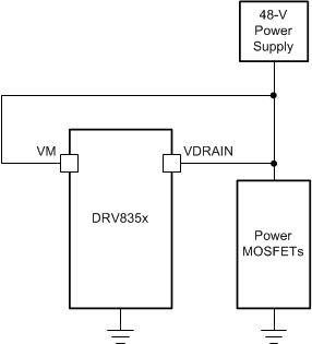
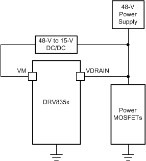
Since the charge pump output is regulated to VVDRAIN + 10.5 V this allows for VM to be supplied either directly from the high voltage motor supply (up to 75 V) to support a single supply system or from a low voltage gate driver power supply derived from a switching or linear regulator to improve the device efficiency or utilize an externally available power supply. Figure 13-11 and Figure 13-12 show examples of the DRV8353M configured in either single supply or dual supply configuration.
 Figure 13-11 Single Supply Example
 Figure 13-12 Dual Supply Example