JAJSVI5 October   2024 DRV8376

ADVANCE INFORMATION  

  1.   1
  2. 特長
  3. アプリケーション
  4. 概要
  5. Device Comparison Table
  6. Pin Configuration and Functions
  7. Specifications
    1. 6.1 Absolute Maximum Ratings
    2. 6.2 ESD Ratings
    3. 6.3 Recommended Operating Conditions
    4. 6.4 Thermal Information
    5. 6.5 Electrical Characteristics
    6. 6.6 SPI Timing Requirements
    7. 6.7 SPI Slave Mode Timings
  8. Detailed Description
    1. 7.1 Overview
    2. 7.2 Functional Block Diagram
    3. 7.3 Feature Description
      1. 7.3.1  Output Stage
      2. 7.3.2  Control Modes
        1. 7.3.2.1 6x PWM Mode (PWM_MODE = 00b or 01b or MODE_SR Pin Tied to AGND or in Hi-Z)
        2. 7.3.2.2 3x PWM Mode (xPWM_MODE = 10b or 11b or MODE_SR Pin is Connected to GVDD or to GVDD with RMODE)
      3. 7.3.3  Device Interface Modes
        1. 7.3.3.1 Serial Peripheral Interface (SPI)
        2. 7.3.3.2 Hardware Interface
      4. 7.3.4  AVDD and GVDD Linear Voltage Regulator
      5. 7.3.5  Charge Pump
      6. 7.3.6  Slew Rate Control
      7. 7.3.7  Cross Conduction (Dead Time)
      8. 7.3.8  Propagation Delay
      9. 7.3.9  Pin Diagrams
        1. 7.3.9.1 Logic Level Input Pin (Internal Pulldown)
        2. 7.3.9.2 Logic Level Input Pin (Internal Pullup)
        3. 7.3.9.3 Open Drain Pin
        4. 7.3.9.4 Push Pull Pin
        5. 7.3.9.5 Four Level Input Pin
      10. 7.3.10 Current Sense Amplifiers
        1. 7.3.10.1 Current Sense Amplifier Operation
      11. 7.3.11 Active Demagnetization
        1. 7.3.11.1 Automatic Synchronous Rectification Mode (ASR Mode)
          1. 7.3.11.1.1 Automatic Synchronous Rectification in Commutation
          2. 7.3.11.1.2 Automatic Synchronous Rectification in PWM Mode
        2. 7.3.11.2 Automatic Asynchronous Rectification Mode (AAR Mode)
      12. 7.3.12 Cycle-by-Cycle Current Limit
        1. 7.3.12.1 Cycle by Cycle Current Limit with 100% Duty Cycle Input
      13. 7.3.13 Protections
        1. 7.3.13.1 VM Supply Undervoltage Lockout (RESET)
        2. 7.3.13.2 AVDD Undervoltage Protection (AVDD_UV)
        3. 7.3.13.3 GVDD Undervoltage Lockout (GVDD_UV)
        4. 7.3.13.4 VCP Charge Pump Undervoltage Lockout (CPUV)
        5. 7.3.13.5 Overvoltage Protections (OV)
        6. 7.3.13.6 Overcurrent Protection (OCP)
          1. 7.3.13.6.1 OCP Latched Shutdown (OCP_MODE = 00b)
          2. 7.3.13.6.2 OCP Automatic Retry (OCP_MODE = 01b)
          3. 7.3.13.6.3 OCP Report Only (OCP_MODE = 10b)
          4. 7.3.13.6.4 OCP Disabled (OCP_MODE = 11b)
        7. 7.3.13.7 Thermal Warning (OTW)
        8. 7.3.13.8 Thermal Shutdown (OTS)
    4. 7.4 Device Functional Modes
      1. 7.4.1 Functional Modes
        1. 7.4.1.1 Sleep Mode
        2. 7.4.1.2 Operating Mode
        3. 7.4.1.3 Fault Reset (CLR_FLT or nSLEEP Reset Pulse)
      2. 7.4.2 DRVOFF functionality
    5. 7.5 SPI Communication
      1. 7.5.1 Programming
        1. 7.5.1.1 SPI Format
    6. 7.6 Register Map
      1. 7.6.1 STATUS Registers
      2. 7.6.2 CONTROL Registers
  9. Application and Implementation
    1. 8.1 Application Information
    2. 8.2 Power Supply Recommendations
      1. 8.2.1 Bulk Capacitance
    3. 8.3 Layout
      1. 8.3.1 Layout Guidelines
      2. 8.3.2 Layout Example
      3. 8.3.3 Thermal Considerations
        1. 8.3.3.1 Power Dissipation
  10. Device and Documentation Support
    1. 9.1 Documentation Support
    2. 9.2 サポート・リソース
    3. 9.3 Trademarks
    4. 9.4 静電気放電に関する注意事項
    5. 9.5 用語集
  11. 10Revision History
  12. 11Mechanical, Packaging, and Orderable Information
    1. 11.1 Package Option Addendum
    2. 11.2 Tape and Reel Information

パッケージ・オプション

メカニカル・データ(パッケージ|ピン)
  • NLG|28
サーマルパッド・メカニカル・データ
発注情報

Slew Rate Control

An adjustable gate-drive current control to the MOSFETs of half-bridges is implemented to achieve the slew rate control. The MOSFET VDS slew rates are a critical factor for optimizing radiated emissions, energy and duration of diode recovery spikes, and switching voltage transients related to parasitics. These slew rates are predominantly determined by the rate of gate charge to internal MOSFETs as shown in Figure 7-10.
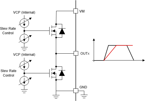
DRV8376 Slew Rate Circuit ImplementationFigure 7-10 Slew Rate Circuit Implementation

The slew rate of each half-bridge can be adjusted by the SLEW pin in the hardware device variant or by using the SLEW bits in the SPI device variant. Each half-bridge can be selected to either of a slew rate setting of 1.1V/ns, 0.5V/ns, 0.25V/ns, or 0.05V/ns. The slew rate is calculated by the rise time and fall time of the voltage on the OUTx pin as shown in Figure 7-11.
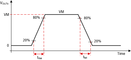
DRV8376 Slew Rate TimingsFigure 7-11 Slew Rate Timings
Note: The SLEW pin is sensed only during power up and the DRV8376H device doesn't support slew rate change during operation. Slew rate can be changed during operation through register write in DRV8376S device. TI recommends not to change the slew rate during operation.