SLOSEC6 August   2024 DRV8434A-Q1

PRODUCTION DATA  

  1.   1
  2. Features
  3. Applications
  4. Description
  5. Pin Configuration and Functions
    1. 4.1 Pin Functions
  6. Specifications
    1. 5.1 Absolute Maximum Ratings
    2. 5.2 ESD Ratings
    3. 5.3 Recommended Operating Conditions
    4. 5.4 Thermal Information
    5. 5.5 Electrical Characteristics
    6. 5.6 STEP and DIR Timing Requirements
      1. 5.6.1 Typical Characteristics
  7. Detailed Description
    1. 6.1 Overview
    2. 6.2 Functional Block Diagram
    3. 6.3 Feature Description
      1. 6.3.1 Stepper Motor Driver Current Ratings
        1. 6.3.1.1 Peak Current Rating
        2. 6.3.1.2 RMS Current Rating
        3. 6.3.1.3 Full-Scale Current Rating
      2. 6.3.2 PWM Motor Drivers
      3. 6.3.3 Microstepping Indexer
      4. 6.3.4 Controlling VREF with an MCU DAC
      5. 6.3.5 Current Regulation and Decay Mode
        1. 6.3.5.1 Smart tune Ripple Control
        2. 6.3.5.2 Blanking time
      6. 6.3.6 Charge Pump
      7. 6.3.7 Linear Voltage Regulators
      8. 6.3.8 Logic Level, Tri-Level and Quad-Level Pin Diagrams
        1. 6.3.8.1 nFAULT and STL_REP Pin
      9. 6.3.9 Protection Circuits
        1. 6.3.9.1 VM Undervoltage Lockout (UVLO)
        2. 6.3.9.2 VCP Undervoltage Lockout (CPUV)
        3. 6.3.9.3 Overcurrent Protection (OCP)
        4. 6.3.9.4 Stall Detection
        5. 6.3.9.5 Open-Load Detection (OL)
        6. 6.3.9.6 Thermal Shutdown (OTSD)
        7.       Fault Condition Summary
    4. 6.4 Device Functional Modes
      1. 6.4.1 Sleep Mode (nSLEEP = 0)
      2.      43
      3. 6.4.2 Disable Mode (nSLEEP = 1, ENABLE = 0)
      4. 6.4.3 Operating Mode (nSLEEP = 1, ENABLE = Hi-Z/1)
      5. 6.4.4 nSLEEP Reset Pulse
      6.      Functional Modes Summary
  8. Application and Implementation
    1. 7.1 Application Information
    2. 7.2 Typical Application
      1. 7.2.1 Design Requirements
      2. 7.2.2 Detailed Design Procedure
        1. 7.2.2.1 Stepper Motor Speed
        2. 7.2.2.2 Current Regulation
        3. 7.2.2.3 Decay Mode
        4. 7.2.2.4 Application Curves
        5. 7.2.2.5 Thermal Application
          1. 7.2.2.5.1 Power Dissipation
          2. 7.2.2.5.2 Conduction Loss
          3. 7.2.2.5.3 Switching Loss
          4. 7.2.2.5.4 Power Dissipation Due to Quiescent Current
          5. 7.2.2.5.5 Total Power Dissipation
          6. 7.2.2.5.6 Device Junction Temperature Estimation
  9. Power Supply Recommendations
    1. 8.1 Bulk Capacitance
  10. Layout
    1. 9.1 Layout Guidelines
    2. 9.2 Layout Example
  11. 10Device and Documentation Support
    1. 10.1 Related Documentation
    2. 10.2 Receiving Notification of Documentation Updates
    3. 10.3 Support Resources
    4. 10.4 Trademarks
    5. 10.5 Electrostatic Discharge Caution
    6. 10.6 Glossary
  12. 11Revision History
  13. 12Mechanical, Packaging, and Orderable Information

パッケージ・オプション

メカニカル・データ(パッケージ|ピン)
サーマルパッド・メカニカル・データ
発注情報

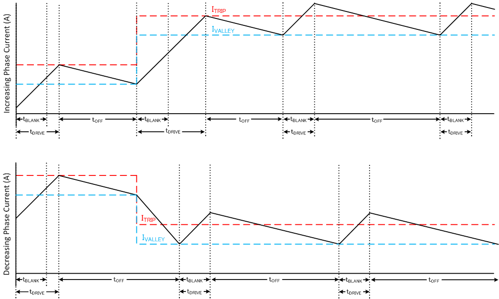
Smart tune Ripple Control

DRV8434A-Q1 Smart tune Ripple Control Decay ModeFigure 6-5 Smart tune Ripple Control Decay Mode

Smart tune Ripple Control operates by setting an IVALLEY level alongside the ITRIP level. When the current level reaches ITRIP, the driver enters slow decay until IVALLEY is reached. In slow decay, both low-side MOSFETs are turned on allowing the current to recirculate. In this mode, off-time varies depending on the current level and operating conditions.

The ripple control method allows tight regulation of the current level increasing motor efficiency and system performance.