JAJSD22B March 2017 – December 2018 DRV8702D-Q1 , DRV8703D-Q1
PRODUCTION DATA.
- 1 特長
- 2 アプリケーション
- 3 概要
- 4 改訂履歴
- 5 Pin Configuration and Functions
- 6 Specifications
-
7 Detailed Description
- 7.1 Overview
- 7.2 Functional Block Diagram
- 7.3
Feature Description
- 7.3.1 Bridge Control
- 7.3.2 MODE Pin
- 7.3.3 nFAULT Pin
- 7.3.4 Current Regulation
- 7.3.5 Amplifier Output (SO)
- 7.3.6 PWM Motor Gate Drivers
- 7.3.7 IDRIVE Pin (DRV8702D-Q1 Only)
- 7.3.8 Dead Time
- 7.3.9 Propagation Delay
- 7.3.10 Overcurrent VDS Monitor
- 7.3.11 VDS Pin (DRV8702D-Q1 Only)
- 7.3.12 Charge Pump
- 7.3.13 Gate Drive Clamp
- 7.3.14
Protection Circuits
- 7.3.14.1 VM Undervoltage Lockout (UVLO2)
- 7.3.14.2 Logic Undervoltage (UVLO1)
- 7.3.14.3 VCP Undervoltage Lockout (CPUV)
- 7.3.14.4 Overcurrent Protection (OCP)
- 7.3.14.5 Gate Driver Fault (GDF)
- 7.3.14.6 Thermal Shutdown (TSD)
- 7.3.14.7 Watchdog Fault (WDFLT, DRV8703D-Q1 Only)
- 7.3.14.8 Reverse Supply Protection
- 7.3.15 Hardware Interface
- 7.4 Device Functional Modes
- 7.5 Programming
- 7.6 Register Maps
- 8 Application and Implementation
- 9 Power Supply Recommendations
- 10Layout
- 11デバイスおよびドキュメントのサポート
- 12メカニカル、パッケージ、および注文情報
パッケージ・オプション
デバイスごとのパッケージ図は、PDF版データシートをご参照ください。
メカニカル・データ(パッケージ|ピン)
- RHB|32
サーマルパッド・メカニカル・データ
発注情報
9.1 Bulk Capacitance Sizing
Bulk capacitance sizing is an important factor in motor drive system design. It is beneficial to have more bulk capacitance, while the disadvantages are increased cost and physical size.
The amount of local capacitance needed depends on a variety of factors including:
- The highest current required by the motor system.
- The capacitance of the power supply and the ability of the power supply to source current.
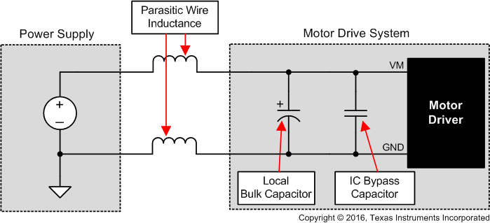
- The amount of parasitic inductance between the power supply and motor system.
- The acceptable voltage ripple.
- The type of motor used (brushed DC, brushless DC, and stepper).
- The motor braking method.
The inductance between the power supply and motor drive system limits the rate that current can change from the power supply. If the local bulk capacitance is too small, the system responds to excessive current demands or dumps from the motor with a change in voltage. When sufficient bulk capacitance is used, the motor voltage remains stable, and high current can be quickly supplied.
The data sheet provides a recommended value, but system-level testing is required to determine the appropriate sized bulk capacitor.
 Figure 59. Example Setup of Motor Drive System With External Power Supply
 The voltage rating for bulk capacitors should be higher than the operating voltage to provide a margin for cases when the motor transfers energy to the supply.