JAJSPW4D February   2011  – March 2021 DRV8801-Q1

PRODUCTION DATA  

  1. 特長
  2. アプリケーション
  3. 概要
  4. Revision History
  5. Pin Configuration and Functions
  6. Specifications
    1. 6.1 Absolute Maximum Ratings
    2. 6.2 ESD Ratings
    3. 6.3 Recommended Operating Conditions
    4. 6.4 Thermal Information
    5. 6.5 Electrical Characteristics
    6. 6.6 Timing Requirements
    7. 6.7 Typical Characteristics
  7. Detailed Description
    1. 7.1 Overview
    2. 7.2 Functional Block Diagram
    3. 7.3 Feature Description
      1. 7.3.1 Power Supervisor
      2. 7.3.2 Bridge Control
        1. 7.3.2.1 MODE 1
        2. 7.3.2.2 MODE 2
      3. 7.3.3 Fast Decay with Synchronous Rectification
      4. 7.3.4 Slow Decay with Synchronous Rectification (Brake Mode)
      5. 7.3.5 Charge Pump
      6. 7.3.6 SENSE
      7. 7.3.7 VPROPI
        1. 7.3.7.1 Connecting VPROPI Output to ADC
      8. 7.3.8 Protection Circuits
        1. 7.3.8.1 VBB Undervoltage Lockout (UVLO)
        2. 7.3.8.2 Overcurrent Protection (OCP)
        3. 7.3.8.3 Overtemperature Warning (OTW)
        4. 7.3.8.4 Overtemperature Shutdown (OTS)
      9. 7.3.9 Thermal Shutdown (TSD)
    4. 7.4 Device Functional Modes
  8. Application and Implementation
    1. 8.1 Application Information
    2. 8.2 Typical Application
      1. 8.2.1 Design Requirements
      2. 8.2.2 Detailed Design Procedure
        1. 8.2.2.1 Motor Voltage
        2. 8.2.2.2 Power Dissipation
        3. 8.2.2.3 Thermal Considerations
          1. 8.2.2.3.1 Junction-to-Ambiant Thermal Impedance (ƟJA)
        4. 8.2.2.4 Motor Current Trip Point
        5. 8.2.2.5 Sense Resistor Selection
        6. 8.2.2.6 Drive Current
      3. 8.2.3 Pulse-Width Modulating
        1. 8.2.3.1 Pulse-Width Modulating ENABLE
        2. 8.2.3.2 Pulse-Width Modulating PHASE
      4. 8.2.4 Application Curves
    3. 8.3 Parallel Configuration
      1. 8.3.1 Parallel Connections
      2. 8.3.2 Non – Parallel Connections
      3. 8.3.3 Wiring nFAULT as Wired OR
      4. 8.3.4 Electrical Considerations
        1. 8.3.4.1 Device Spacing
        2. 8.3.4.2 Recirculation Current Handling
        3. 8.3.4.3 Sense Resistor Selection
        4. 8.3.4.4 Maximum System Current
  9. Power Supply Recommendations
    1. 9.1 Bulk Capacitance
  10. 10Layout
    1. 10.1 Layout Guidelines
    2. 10.2 Layout Example
  11. 11Device and Documentation Support
    1. 11.1 Documentation Support
      1. 11.1.1 Related Documentation
    2. 11.2 Receiving Notification of Documentation Updates
    3. 11.3 サポート・リソース
    4. 11.4 Trademarks
    5. 11.5 静電気放電に関する注意事項
    6. 11.6 用語集
  12. 12Mechanical, Packaging, and Orderable Information

パッケージ・オプション

メカニカル・データ(パッケージ|ピン)
サーマルパッド・メカニカル・データ
発注情報

Bulk Capacitance

Having appropriate local bulk capacitance is an important factor in motor drive system design. It is generally beneficial to have more bulk capacitance, while the disadvantages are increased cost and physical size.

The amount of local capacitance needed depends on a variety of factors, including:

  • The highest current required by the motor system.
  • The capacitance of the power supply and its ability to source current.
  • The amount of parasitic inductance between the power supply and motor systems.
  • The acceptable voltage ripple.
  • The type of motor used (Brushed DC, Brushless DC, Stepper).
  • The motor braking method.

The inductance between the power supply and motor drive system will limit the rate current can change from the power supply. If the local bulk capacitance is too small, the system will respond to excessive current demands or dumps from the motor with a change in voltage. When adequate bulk capacitance is used, the motor voltage remains stable and high current can be quickly supplied.

The data sheet generally provides a recommended value, but system-level testing is required to determine the appropriate sized bulk capacitor.
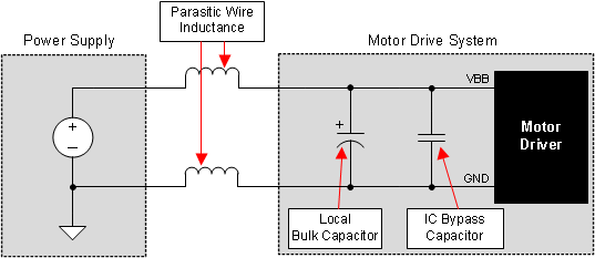
GUID-9519CC76-66F3-4FD6-946D-6809F0BBEDE4-low.gifFigure 9-1 Example Setup of Motor Drive System With External Power Supply