SLVSCI2A June 2014 – June 2014 DRV8802-Q1
PRODUCTION DATA.
- 1 Features
- 2 Applications
- 3 Description
- 4 Revision History
- 5 Pin Configuration and Functions
- 6 Specifications
- 7 Detailed Description
- 8 Application and Implementation
- 9 Power Supply Recommendations
- 10Layout
- 11Device and Documentation Support
- 12Mechanical, Packaging, and Orderable Information
パッケージ・オプション
メカニカル・データ(パッケージ|ピン)
- PWP|28
サーマルパッド・メカニカル・データ
- PWP|28
発注情報
1 Features
- Qualified for Automotive Applications
- AEC-Q100 Qualified With the Following Results
- Device Temperature Grade 1: –40°C to 125°C Ambient Operating Temperature
- Device HBM ESD Classification Level 2
- Device CDM ESD Classification Level C4B
- Dual H-Bridge Current-Control Motor Driver
- Drives Two DC Motors
- Brake Mode
- Two-Bit Winding Current Control Allows Up to 4 Current Levels
- Low MOSFET On-Resistance
- 1.6-A Maximum Drive Current at 24 V, 25°C
- Built-In 3.3-V Reference Output
- Industry Standard Parallel Digital Control
Interface - 8-V to 45-V Operating Supply Voltage Range
- Thermally Enhanced Surface Mount Package
2 Applications
- Automotive HVAC
- Automotive Valves
- Automotive Infotainment
3 Description
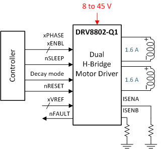
The DRV8802-Q1 device provides an integrated motor driver solution for automotive applications. The device has two H-bridge drivers, and is intended to drive DC motors. The output driver block for each consists of N-channel power MOSFET’s configured as H-bridges to drive the motor windings. The DRV8802-Q1 device can supply up to 1.6-A peak or 1.1-A RMS output current (with proper heatsinking at 24 V and 25°C) per H-bridge.
A simple parallel digital control interface is compatible with industry-standard devices. Decay mode is programmable to allow braking or coasting of the motor when disabled.
Internal shutdown functions are provided for over current protection, short circuit protection, under voltage lockout and overtemperature.
The DRV8802-Q1 device is available in a 28-pin HTSSOP package with PowerPAD™ (Eco-friendly: RoHS & no Sb/Br).
Device Information(1)
| PART NUMBER | PACKAGE | BODY SIZE (NOM) |
|---|---|---|
| DRV8802-Q1 | HTSSOP (28) | 9.70 mm × 4.40 mm |
- For all available packages, see the orderable addendum at the end of the datasheet.
Simplified Application Diagram