SLVSAW4F July 2011 – December 2015 DRV8804
PRODUCTION DATA.
- 1 Features
- 2 Applications
- 3 Description
- 4 Revision History
- 5 Pin Configuration and Functions
- 6 Specifications
- 7 Detailed Description
- 8 Application and Implementation
- 9 Power Supply Recommendations
- 10Layout
- 11Device and Documentation Support
- 12Mechanical, Packaging, and Orderable Information
パッケージ・オプション
メカニカル・データ(パッケージ|ピン)
サーマルパッド・メカニカル・データ
- PWP|16
発注情報
10 Layout
10.1 Layout Guidelines
The voltage rating for bulk capacitors should be higher than the operating voltage, to provide margin for cases when the motor transfers energy to the supply.
- Small-value capacitors should be ceramic, and placed closely to device pins.
- The high-current device outputs should use wide metal traces.
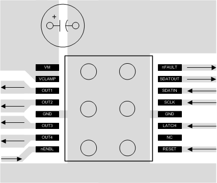
The device thermal pad should be soldered to the PCB top-layer ground plane. Multiple vias should be used to connect to a large bottom-layer ground plane. The use of large metal planes and multiple vias help dissipate the I2 × RDS(on) heat that is generated in the device.
10.2 Layout Example
 Figure 13. Layout Recommendation
10.3 Thermal Considerations
The DRV8804 has thermal shutdown (TSD) as described in Thermal Shutdown (TSD). If the die temperature exceeds approximately 150°C, the device will be disabled until the temperature drops to a safe level.
Any tendency of the device to enter TSD is an indication of either excessive power dissipation, insufficient heatsinking, or too high an ambient temperature.
10.3.1 Power Dissipation
Power dissipation in the DRV8804 is dominated by the power dissipated in the output FET resistance, or RDS(ON). Average power dissipation of each FET when running a static load can be roughly estimated by Equation 2.

where
- P is the power dissipation of one FET
- RDS(ON) is the resistance of each FET
- IOUT is equal to the average current drawn by the load
Note that at start-up and fault conditions this current is much higher than normal running current; these peak currents and their duration also must be taken into consideration. When driving more than one load simultaneously, the power in all active output stages must be summed.
The maximum amount of power that can be dissipated in the device is dependent on ambient temperature and heatsinking.
Note that RDS(ON) increases with temperature, so as the device heats, the power dissipation increases. This must be taken into consideration when sizing the heatsink.
10.3.2 Heatsinking
The DRV8804DW package uses a standard SOIC outline, but has the center pins internally fused to the die pad to more efficiently remove heat from the device. The two center leads on each side of the package should be connected together to as large a copper area on the PCB as is possible to remove heat from the device. If the copper area is on the opposite side of the PCB from the device, thermal vias are used to transfer the heat between top and bottom layers.
In general, the more copper area that can be provided, the more power can be dissipated.
The DRV8804PWP package uses an HTSSOP package with an exposed PowerPAD™. The PowerPAD package uses an exposed pad to remove heat from the device. For proper operation, this pad must be thermally connected to copper on the PCB to dissipate heat. On a multi-layer PCB with a ground plane, this can be accomplished by adding a number of vias to connect the thermal pad to the ground plane. On PCBs without internal planes, copper area can be added on either side of the PCB to dissipate heat. If the copper area is on the opposite side of the PCB from the device, thermal vias are used to transfer the heat between top and bottom layers.
For details about how to design the PCB, see TI Application Report, PowerPAD Thermally Enhanced Package (SLMA002), and TI Application Brief, PowerPAD Made Easy (SLMA004), available at www.ti.com.