-
DRV8837C 1A低電圧、Hブリッジ・ドライバ
パッケージ・オプション
メカニカル・データ(パッケージ|ピン)
- DSG|8
サーマルパッド・メカニカル・データ
- DSG|8
発注情報
DRV8837C 1A低電圧、Hブリッジ・ドライバ
1 特長
- Hブリッジ・モータ・ドライバ
- DCモータまたは他の負荷を駆動
- 低いMOSFETオン抵抗: HS + LS 1Ω
- 最大1Aの駆動電流
- 動作電源電圧範囲: 0~11V
- 標準PWMインターフェイス(IN1/IN2)
- 低消費電力のスリープ・モード、スリープ時の最大電流120nA
- nSLEEPピン
- 小さなパッケージと占有面積
- 8 WSON (サーマル・パッド付き)
- 2.0×2.0mm
- 保護機能
- VCC低電圧誤動作防止(UVLO)
- 過電流保護(OCP)
- サーマル・シャットダウン(TSD)
2 アプリケーション
- カメラ
- DSLRレンズ
- コンシューマ製品
- 玩具
- ロボティクス
- 医療機器
3 概要
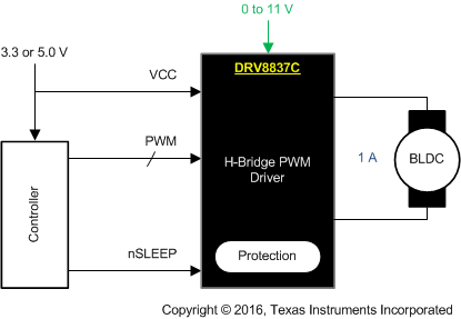
DRV8837Cデバイスは、カメラ、コンシューマ製品、玩具、その他低電圧またはバッテリ駆動のモーション制御用途に使用される内蔵用モータ・ドライバ・ソリューションです。このデバイスは、1つのDCモータ、またはソレノイドなど他のデバイスを駆動できます。出力ドライバ・ブロックには、モータ巻線を駆動するHブリッジとして構成されたNチャネルのパワーMOSFETが搭載されています。内部のチャージ・ポンプにより、必要なゲート・ドライブ電圧が生成されます。
DRV8837Cデバイスは、最大1Aの出力電流を供給できます。このデバイスは、モータの電源電圧0~11Vで動作し、制御ロジックは1.8V~5Vレールで動作できます。
DRV8837Cデバイスには、PWM (IN/IN)入力インターフェイスが搭載されています。
過電流保護、短絡保護、低電圧誤動作防止、および過熱保護のために、内部シャットダウン機能が用意されています。
製品情報(1)
| 型番 | パッケージ | 本体サイズ(公称) |
|---|---|---|
| DRV8837C | WSON (8) | 2.00mm×2.00mm |
- 利用可能なすべてのパッケージについては、このデータシートの末尾にある注文情報を参照してください。
DRV8837Cの簡略ブロック図
5 Pin Configuration and Functions
Pin Functions
| PIN | TYPE | DESCRIPTION | |
|---|---|---|---|
| NAME | NO. | ||
| POWER AND GROUND | |||
| GND | 4 | PWR | Device ground This pin must be connected to the PCB ground. |
| VCC | 8 | PWR | Logic power supply Bypass this pin to the GND pin with a 0.1-µF ceramic capacitor rated for VCC. |
| VM | 1 | PWR | Motor power supply Bypass this pin to the GND pin with a 0.1-µF ceramic capacitor rated for VM. |
| CONTROL | |||
| IN1 | 6 | I | IN1 input |
| IN2 | 5 | I | IN2 input |
| nSLEEP | 7 | I | Sleep mode input When this pin is in logic low, the device enters low-power sleep mode. The device operates normally when this pin is logic high. The pin has an internal pulldown resistor to GND. |
| OUTPUT | |||
| OUT1 | 2 | O | Motor output Connect this pin to the motor winding. |
| OUT2 | 3 | O | |
6 Specifications
6.1 Absolute Maximum Ratings
Over operating free-air temperature range (unless otherwise noted)(1)(2)| MIN | MAX | UNIT | ||
|---|---|---|---|---|
| Motor power-supply voltage | VM | –0.3 | 12 | V |
| Logic power-supply voltage | VCC | –0.3 | 7 | V |
| Control pin voltage | IN1, IN2, nSLEEP | –0.5 | 7 | V |
| Peak drive current | OUT1, OUT2 | Internally limited | A | |
| Operating virtual junction temperature, TJ | –40 | 150 | ºC | |
| Storage temperature, Tstg | –60 | 150 | ºC | |
6.2 ESD Ratings
| VALUE | UNIT | |||
|---|---|---|---|---|
| V(ESD) | Electrostatic discharge | Human-body model (HBM), per ANSI/ESDA/JEDEC JS-001(1) | ±4000 | V |
| Charged-device model (CDM), per JEDEC specification JESD22-C101(2) | ±1000 | |||
6.3 Recommended Operating Conditions
Over operating free-air temperature range (unless otherwise noted)| MIN | MAX | UNIT | ||
|---|---|---|---|---|
| VVM | Motor power-supply voltage | 0 | 11 | V |
| VCC | Logic power-supply voltage | 1.8 | 7 | V |
| IOUT | Motor peak current | 0 | 1 | A |
| fPWM | Externally applied PWM frequency | 0 | 250 | kHz |
| VLOGIC | Logic level input voltage | 0 | 5.5 | V |
| TA | Operating ambient temperature | –40 | 85 | °C |
6.4 Thermal Information
over operating free-air temperature range (unless otherwise noted)| THERMAL METRIC (1) | DRV8837C | UNIT | |
|---|---|---|---|
| DSG (WSON) | |||
| 8 PINS | |||
| RθJA | Junction-to-ambient thermal resistance | 60.9 | °C/W |
| RθJC(top) | Junction-to-case (top) thermal resistance | 71.4 | °C/W |
| RθJB | Junction-to-board thermal resistance | 32.2 | °C/W |
| ψJT | Junction-to-top characterization parameter | 1.6 | °C/W |
| ψJB | Junction-to-board characterization parameter | 32.8 | °C/W |
| RθJC(bot) | Junction-to-case (bottom) thermal resistance | 9.8 | °C/W |
6.5 Electrical Characteristics
TA = 25°C, over recommended operating conditions unless otherwise noted| PARAMETER | TEST CONDITIONS | MIN | TYP | MAX | UNIT | |
|---|---|---|---|---|---|---|
| POWER SUPPLIES (VM, VCC) | ||||||
| VVM | VM operating voltage | 0 | 11 | V | ||
| IVM | VM operating supply current | VVM = 5 V; VCC = 3 V; No PWM |
40 | 100 | μA | |
| VVM = 5 V; VCC = 3 V; 50 kHz PWM |
0.8 | 1.5 | mA | |||
| IVMQ | VM sleep mode supply current | VVM = 5 V; VCC = 3 V; nSLEEP = 0 |
30 | 95 | nA | |
| VCC | VCC operating voltage | 1.8 | 7 | V | ||
| IVCC | VCC operating supply current | VVM = 5 V; VCC = 3 V; No PWM |
300 | 500 | μA | |
| VVM = 5 V; VCC = 3 V; 50 kHz PWM |
0.7 | 1.5 | mA | |||
| IVCCQ | VCC sleep mode supply current | VVM = 5 V; VCC = 3 V; nSLEEP = 0 |
5 | 25 | nA | |
| CONTROL INPUTS (IN1/PH, IN2/EN, nSLEEP) | ||||||
| VIL | Input logic-low voltage | 0.25 × VCC | V | |||
| VIH | Input logic-high voltage | 0.5 × VCC | V | |||
| VHYS | Input logic hysteresis | 0.08 × VCC | V | |||
| IIL | Input logic-low current | VINx = 0 V | –5 | 5 | μA | |
| IIH | Input logic-high current | VINx = 3.3 V | 50 | μA | ||
| RPD | Pulldown resistance | 100 | kΩ | |||
| MOTOR DRIVER OUTPUTS (OUT1, OUT2) | ||||||
| RDS(ON) | HS + LS FET on-resistance | VVM = 5 V; VCC = 3.3 V; IO = 200 mA; TJ = 25°C |
1000 | mΩ | ||
| IOFF | Off-state leakage current | VOUTx = 0 V | –200 | 200 | nA | |
| PROTECTION CIRCUITS | ||||||
| VUVLO | VCC undervoltage lockout | VCC falling | 1.7 | V | ||
| VCC rising | 1.8 | V | ||||
| IOCP | Overcurrent protection trip level | 1.2 | A | |||
| tDEG | Overcurrent deglitch time | 1 | μs | |||
| tRETRY | Overcurrent retry time | 1 | ms | |||
| TTSD (1) | Thermal shutdown temperature | Die temperature TJ | 150 | 160 | 180 | °C |
6.6 Timing Requirements
TA = 25°C, VVM = 5 V, VCC = 3 V, RL = 20 Ω| NO. | MIN | MAX | UNIT | |||
|---|---|---|---|---|---|---|
| 1 | t7 | Output enable time | See Figure 1. | 300 | ns | |
| 2 | t8 | Output disable time | 300 | ns | ||
| 3 | t9 | Delay time, INx high to OUTx high | 160 | ns | ||
| 4 | t10 | Delay time, INx low to OUTx low | 160 | ns | ||
| 5 | t11 | Output rise time | 20 | 188 | ns | |
| 6 | t12 | Output fall time | 20 | 188 | ns | |
| — | twake | Wake time, nSLEEP rising edge to part active | 30 | μs | ||
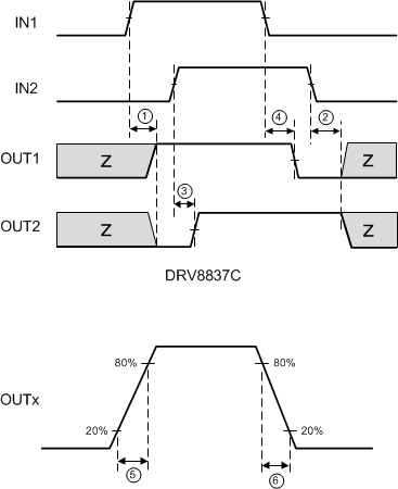 Figure 1. Input and Output Timing for DRV8837C
6.7 Typical Characteristics
Plots generated using characterization data.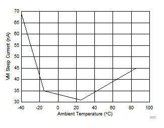
| VVM = 5 V | VCC = 3 V |
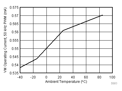
| VVM = 5 V | VCC = 3 V |
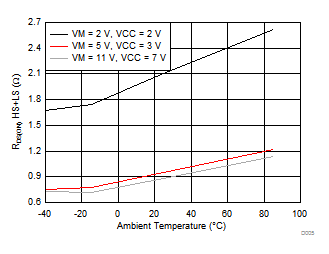 Figure 6. HS + LS RDS(ON) vs Ambient Temperature

| VVM = 5 V | VCC = 3 V |
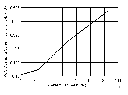
| VVM = 5 V | VCC = 3 V |
7 Detailed Description
7.1 Overview
The DRV8837C device is an H-bridge driver that can drive one DC motor or other devices like solenoids. The outputs are controlled using a PWM interface (IN1/IN2).
A low-power sleep mode is included, which can be enabled using the nSLEEP pin.
This device greatly reduces the component count of motor driver systems by integrating the necessary driver FETs and FET control circuitry into a single device. In addition, the DRV8837C device adds protection features beyond traditional discrete implementations: undervoltage lockout, overcurrent protection, and thermal shutdown.
7.2 Functional Block Diagram

7.3 Feature Description
7.3.1 Bridge Control
The DRV8837C device is controlled using a PWM input interface, also called an IN/IN interface. Each output is controlled by a corresponding input pin.
Table 1 shows the logic for the DRV8837C device.
Table 1. DRV8837C Device Logic
| nSLEEP | IN1 | IN2 | OUT1 | OUT2 | FUNCTION (DC MOTOR) |
|---|---|---|---|---|---|
| 0 | X | X | Z | Z | Coast |
| 1 | 0 | 0 | Z | Z | Coast |
| 1 | 0 | 1 | L | H | Reverse |
| 1 | 1 | 0 | H | L | Forward |
| 1 | 1 | 1 | L | L | Brake |
7.3.2 Sleep Mode
If the nSLEEP pin is brought to a logic-low state, the DRV8837C device enters a low-power sleep mode. In this state, all unnecessary internal circuitry is powered down.
7.3.3 Power Supplies and Input Pins
The input pins can be driven within the recommended operating conditions with or without the VCC, VM, or both power supplies present. No leakage current path exists to the supply. Each input pin has a weak pulldown resistor (approximately 100 kΩ) to ground.
The VCC and VM supplies can be applied and removed in any order. When the VCC supply is removed, the device enters a low-power state and draws very little current from the VM supply. The VCC and VM pins can be connected together if the supply voltage is between 1.8 and 7 V.
The VM voltage supply does not have any undervoltage-lockout protection (UVLO). As long as VCC > 1.8 V, the internal device logic remains active which means that the VM pin voltage can drop to 0 V, however, the load may not be sufficiently driven at low VM voltages.
7.3.4 Protection Circuits
The DRV8837C is fully protected against VCC undervoltage, overcurrent, and overtemperature events.
-
VCC undervoltage lockout If at any time the voltage on the VCC pin falls below the undervoltage lockout threshold voltage, all FETs in the H-bridge are disabled. Operation resumes when the VCC pin voltage rises above the UVLO threshold.
-
Overcurrent protection (OCP) An analog current-limit circuit on each FET limits the current through the FET by removing the gate drive. If this analog current limit persists for longer than tDEG, all FETs in the H-bridge are disabled. Operation resumes automatically after tRETRY has elapsed. Overcurrent conditions are detected on both the high-side and low-side devices. A short to the VM pin, GND, or from the OUT1 pin to theOUT2 pin results in an overcurrent condition.
-
Thermal shutdown (TSD) If the die temperature exceeds safe limits, all FETs in the H-bridge are disabled. After the die temperature falls to a safe level, operation automatically resumes.
Table 2. Fault Behavior
| FAULT | CONDITION | H-BRIDGE | RECOVERY |
|---|---|---|---|
| VCC undervoltage (UVLO) | VCC < 1.7 V | Disabled | VCC > 1.8 V |
| Overcurrent (OCP) | IOUT > 1.2 A (MIN) | Disabled (retries automatically) | tRETRY elapses |
| Thermal Shutdown (TSD) | TJ > 150°C (MIN) | Disabled (retries automatically) | TJ < 150°C |
7.4 Device Functional Modes
The DRV8837C device is active unless the nSLEEP pin is brought logic low. In sleep mode the H-bridge FETs are disabled Hi-Z. The DRV8837C device is brought out of sleep mode automatically if nSLEEP is brought logic high.
The H-bridge outputs are disabled during undervoltage lockout, overcurrent, and overtemperature fault conditions.
Table 3. Operation Modes
| MODE | CONDITION | H-BRIDGE |
|---|---|---|
| Operating | nSLEEP pin = 1 | Operating |
| Sleep mode | nSLEEP pin = 0 | Disabled |
| Fault encountered | Any fault condition met | Disabled (retries automatically) |