SLVSCH4 July 2014 DRV8842-EP
PRODUCTION DATA.
- 1 Features
- 2 Applications
- 3 Description
- 4 Simplified Schematic
- 5 Revision History
- 6 Pin Configuration and Functions
- 7 Specifications
- 8 Detailed Description
- 9 Application and Implementation
- 10Power Supply Recommendations
- 11Layout
- 12Device and Documentation Support
- 13Mechanical, Packaging, and Orderable Information
パッケージ・オプション
メカニカル・データ(パッケージ|ピン)
- PWP|28
サーマルパッド・メカニカル・データ
- PWP|28
発注情報
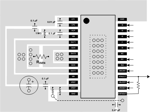
11 Layout
11.1 Layout Guidelines
The VM pins should be bypassed to GND using low-ESR ceramic bypass capacitors with a recommended value of 0.1-μF rated for VM. This capacitor should be placed as close to the VM pins as possible with a thick trace or ground plane connection to the device GND pin.
The VM pins must be bypassed to ground using an appropriate bulk capacitor. This component may be an electrolytic and should be located close to the DRV8842-EP.
A low-ESR ceramic capacitor must be placed in between the CPL and CPH pins. TI recommends a value of 0.01-μF rated for VM. Place this component as close to the pins as possible.
A low-ESR ceramic capacitor must be placed in between the VM and VCP pins. TI recommends a value of
0.1-μF rated for 16 V. Place this component as close to the pins as possible. Also, place a 1-MΩ resistor between VCP and VM.
Bypass V3P3 to ground with a ceramic capacitor rated 6.3 V. Place this bypass capacitor as close to the pin as possible.
11.2 Layout Example