SLVSBA2D July 2012 – May 2016 DRV8844
PRODUCTION DATA.
- 1 Features
- 2 Applications
- 3 Description
- 4 Revision History
- 5 Pin Configuration and Functions
- 6 Specifications
- 7 Detailed Description
- 8 Application and Implementation
- 9 Power Supply Recommendations
- 10Layout
- 11Device and Documentation Support
- 12Mechanical, Packaging, and Orderable Information
パッケージ・オプション
メカニカル・データ(パッケージ|ピン)
- PWP|28
サーマルパッド・メカニカル・データ
- PWP|28
発注情報
7 Detailed Description
7.1 Overview
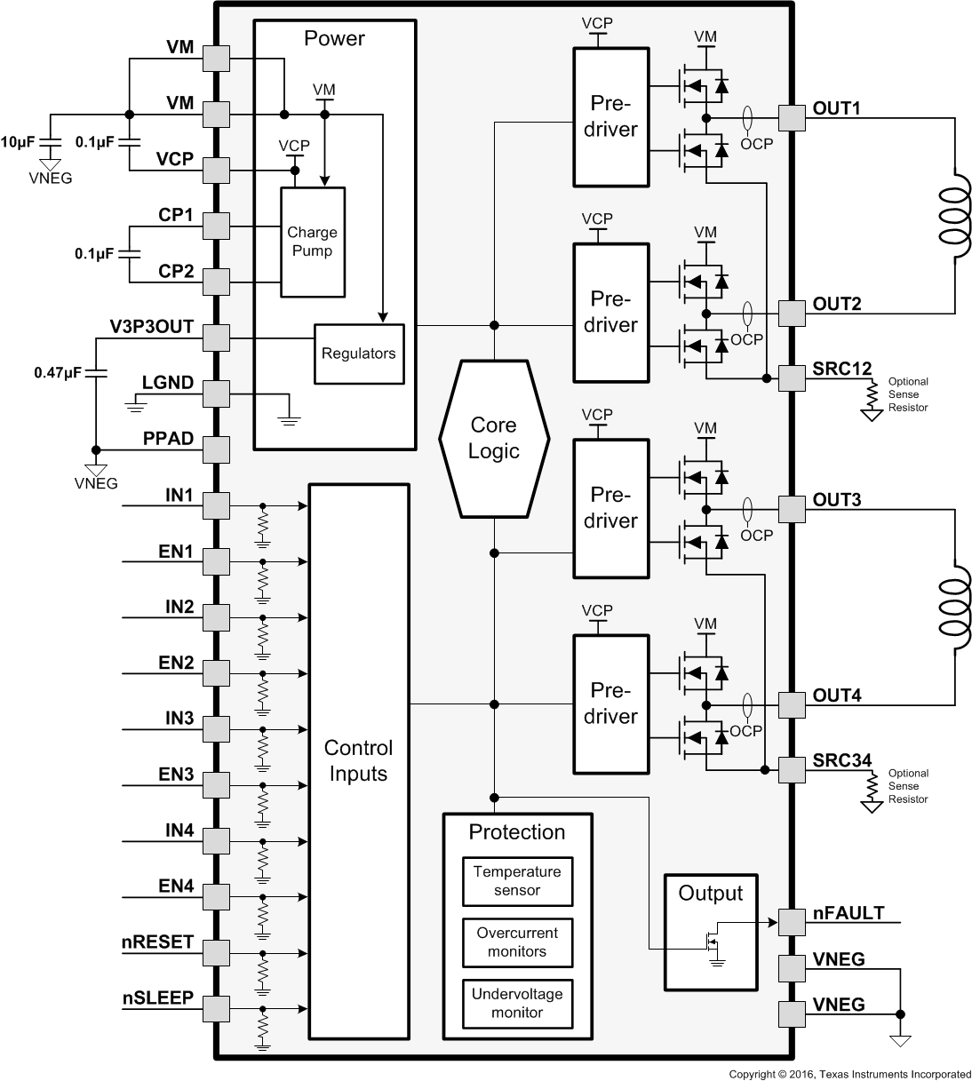
The DRV8844 integrates four independent 2.5-A half-H bridges, protection circuits, sleep mode, and fault reporting. Its single power supply supports a wide 8 to 60 V, making it well-suited for motor drive applications, including brushed DC, steppers, and solenoids.
7.3 Feature Description
7.3.1 Output Stage
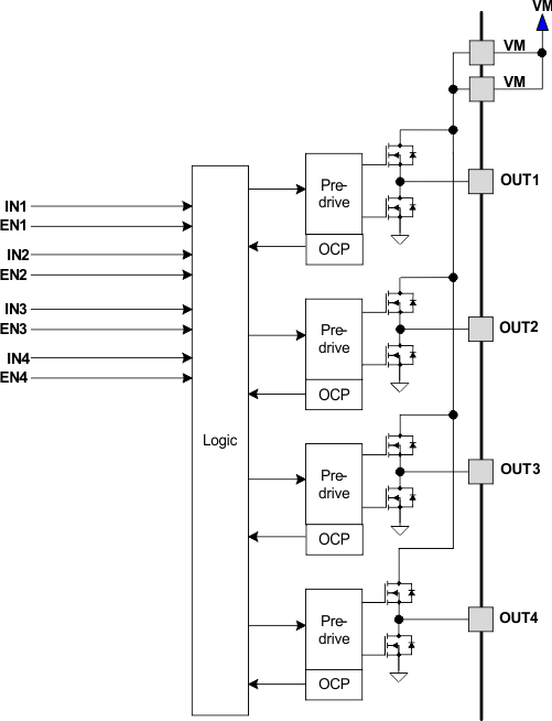
The DRV8844 contains four 1/2-H-bridge drivers using N-channel MOSFETs. A block diagram of the output circuitry is shown in Figure 5.
 Figure 5. Motor Control Circuitry
The output pins are driven between VM and VNEG. VNEG is normally ground for single supply applications, and a negative voltage for dual supply applications.
Note that there are multiple VM motor power supply pins. All VM pins must be connected together to the motor supply voltage.
7.3.2 Logic Inputs
The logic inputs and nFAULT output are referenced to the LGND pin. This pin would be connected to the logic ground of the source of the logic signals (for example, microcontroller). This allows LGND to be at a different voltage than VNEG; for example, the designer can drive a load with bipolar power supplies by driving VM with +24 V and VNEG with -24 V, and connect LGND to 0 V (ground).
7.3.3 Bridge Control
The INx input pins directly control the state (high or low) of the OUTx outputs; the ENx input pins enable or disable the OUTx driver. Table 1 shows the logic.
Table 1. H-Bridge Logic
| INx | ENx | OUTx |
|---|---|---|
| X | 0 | Z |
| 0 | 1 | L |
| 1 | 1 | H |
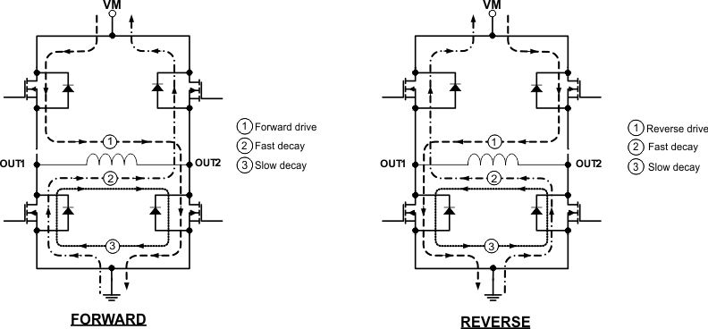
The inputs can also be used for PWM control of, for example, the speed of a DC motor. When controlling a winding with PWM, when the drive current is interrupted, the inductive nature of the motor requires that the current must continue to flow. This is called recirculation current. To handle this recirculation current, the H-bridge can operate in two different states, fast decay or slow decay. In fast decay mode, the H-bridge is disabled and recirculation current flows through the body diodes; in slow decay, the motor winding is shorted.
To PWM using fast decay, the PWM signal is applied to the ENx pin; to use slow decay, the PWM signal is applied to the INx pin. Table 2 is an example of driving a DC motor using OUT1 and OUT2 as an H-bridge:
Table 2. PWM Function
| IN1 | EN1 | IN2 | EN2 | FUNCTION |
|---|---|---|---|---|
| PWM | 1 | 0 | 1 | Forward PWM, slow decay |
| 0 | 1 | PWM | 1 | Reverse PWM, slow decay |
| 1 | PWM | 0 | PWM | Forward PWM, fast decay |
| 0 | PWM | 1 | PWM | Reverse PWM, fast decay |
Figure 6 shows the current paths in different drive and decay modes:
 Figure 6. Current Paths
7.3.4 Charge Pump
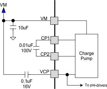
Because the output stages use N-channel FETs, a gate drive voltage higher than the VM power supply is needed to fully enhance the high-side FETs. The DRV8844 integrates a charge pump circuit that generates a voltage above the VM supply for this purpose.
The charge pump requires two external capacitors for operation. Refer to the block diagram and pin descriptions for details on these capacitors (value, connection, and so forth).
The charge pump is shut down when nSLEEP is low.
 Figure 7. Charge Pump
7.3.5 Protection Circuits
The DRV8844 is fully protected against undervoltage, overcurrent and overtemperature events.
7.3.5.1 Overcurrent Protection (OCP)
An analog current limit circuit on each FET limits the current through the FET by removing the gate drive. If this analog current limit persists for longer than the OCP deglitch time, the channel experiencing the overcurrent will be disabled and the nFAULT pin will be driven low. The driver will remain off until either RESET is asserted or VM power is cycled.
Overcurrent conditions on both high and low side devices; i.e., a short to ground, supply, or across the motor winding will all result in an overcurrent shutdown.
7.3.5.2 Thermal Shutdown (TSD)
If the die temperature exceeds safe limits, all FETs in the H-bridge will be disabled and the nFAULT pin will be driven low. Once the die temperature has fallen to a safe level operation will automatically resume.
7.3.5.3 Undervoltage Lockout (UVLO)
If at any time the voltage on the VM pins falls below the undervoltage lockout threshold voltage, all outputs will be disabled, internal logic will be reset, and the nFAULT pin will be driven low. Operation will resume when VM rises above the UVLO threshold.
7.4 Device Functional Modes
7.4.1 nRESET and nSLEEP Operation
The nRESET pin, when driven active low, resets the internal logic. It also disables the H-bridge drivers. All inputs are ignored while nRESET is active.
Driving nSLEEP low will put the device into a low power sleep state. In this state, the H-bridges are disabled, the gate drive charge pump is stopped and all internal clocks are stopped. In this state all inputs are ignored until nSLEEP returns inactive high. When returning from sleep mode, some time (approximately 1 ms) needs to pass before the motor driver becomes fully operational. Note that nRESET and nSLEEP have internal pulldown resistors of approximately 100 kΩ. These signals need to be driven to logic high for device operation.
The V3P3OUT LDO regulator remains operational in sleep mode.
