JAJSFZ9B October 2017 – January 2021 DRV8873-Q1
PRODUCTION DATA
- 1 特長
- 2 アプリケーション
- 3 概要
- 4 Revision History
- 5 Pin Configuration and Functions
- 6 Specifications
-
7 Detailed Description
- 7.1 Overview
- 7.2 Functional Block Diagram
- 7.3 Feature Description
- 7.4 Device Functional Modes
- 7.5 Programming
- 7.6 Register Maps
- 8 Application and Implementation
- 9 Power Supply Recommendations
- 10Layout
- 11Device and Documentation Support
- 12Mechanical, Packaging, and Orderable Information
パッケージ・オプション
メカニカル・データ(パッケージ|ピン)
- PWP|24
サーマルパッド・メカニカル・データ
- PWP|24
発注情報
8.2.1.2 Drive Current and Power Dissipation
The current path is through the high-side sourcing power driver, motor winding, and low-side sinking power driver. The amount of current the device can drive depends on the power dissipation without going into thermal shutdown. The amount of current that can be power dissipation losses in one source and sink power driver are calculated in Equation 2.
The IOUT current is equal to the average current drawn by the DC motor. At 25°C ambient temperature, the power dissipation becomes (2.5 A)2 × (150 mΩ) = 0.94 W.
The temperature that the device reaches depends on the thermal resistance to the air and PCB. Soldering the device PowerPAD to the PCB ground plane, with vias to the top and bottom board layers, is important to dissipate heat into the PCB and reduce the device temperature. In the example used here, the device had an effective thermal resistance RθJA of 27.8°C/W. The junction temperature TJ value becomes as shown in Equation 3.
The values of RDS(on) increases with temperature, so as the device heats, the power dissipation increases. This fact must be taken into consideration when sizing the heatsink.
At start-up and fault conditions, the current flowing through the motor is much higher than normal running current; these peak currents and their duration must also be considered. High PWM frequency also results in higher switching losses. Typically, switching the inputs at 100 kHz compared to 10 kHz causes 20% more power loss in heat.
Power dissipation in the device is dominated by the power dissipated of the internal MOSFET resistance. The maximum amount of power that can be dissipated in the device is dependent on ambient temperature and heatsinking.
Total power dissipation for the device is composed of three main components. These are the quiescent supply current dissipation, the power MOSFET switching losses, and the power MOSFET RDS(ON) (conduction) losses. While other factors may contribute additional power losses, these other items are typically insignificant compared to the three main items.
PVM can be calculated from the nominal supply voltage (VM) and the supply current (IVM) in active mode.
PSW can be calculated from the nominal supply voltage (VM), average output current (IRMS), switching frequency (fPWM) and the device output rise and fall times (tSR) time specifications.
Therefore, total power dissipation (PTOT) at 25°C ambient temperature becomes = PVM + PSW + PD = 67.5 mW + 0.34 W + 0.94 W = 1.35 W
PTOT makes the junction temperature (TJ) of the device to be
The power dissipation from power MOSFET switching losses and quiescent supply current dissipation results is approximately 12°C rise in the junction temperature (different between Equation 9 and Equation 3). Care must be taken when doing the PCB layout and heatsinking the motor driver device so that the thermal characteristics are properly managed.
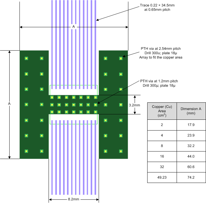
 Figure 8-2 PCB Model (4-Layer PCB Shown, 2-Layer PCB Has No Vias)
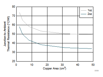
 Figure 8-3 4-Layer PCB Junction-to-Ambient Thermal Resistance vs Copper Area
 Figure 8-5 2-Layer PCB (No Vias) Junction-to-Ambient Thermal Resistance vs Copper Area
 Figure 8-4 4-Layer PCB Junction-to-Board Characterization Parameter vs Copper Area
 Figure 8-6 2-Layer PCB (No Vias) Junction-to-Board Characterization Parameter vs Copper Area