JAJSFZ9B October   2017  – January 2021 DRV8873-Q1

PRODUCTION DATA  

  1. 特長
  2. アプリケーション
  3. 概要
  4. Revision History
  5. Pin Configuration and Functions
    1.     Pin Functions
  6. Specifications
    1. 6.1 Absolute Maximum Ratings
    2. 6.2 ESD Ratings
    3. 6.3 Recommended Operating Conditions
    4. 6.4 Thermal Information
    5. 6.5 Electrical Characteristics
    6. 6.6 SPI Timing Requirements
    7. 6.7 Typical Characteristics
  7. Detailed Description
    1. 7.1 Overview
    2. 7.2 Functional Block Diagram
    3. 7.3 Feature Description
      1. 7.3.1 Bridge Control
        1. 7.3.1.1 Control Modes
        2. 7.3.1.2 Half-Bridge Operation
        3. 7.3.1.3 22
        4. 7.3.1.4 Internal Current Sense and Current Regulation
        5. 7.3.1.5 Slew-Rate Control
        6. 7.3.1.6 Dead Time
        7. 7.3.1.7 Propagation Delay
        8. 7.3.1.8 nFAULT Pin
        9. 7.3.1.9 nSLEEP as SDO Reference
      2. 7.3.2 Motor Driver Protection Circuits
        1. 7.3.2.1 VM Undervoltage Lockout (UVLO)
        2. 7.3.2.2 VCP Undervoltage Lockout (CPUV)
        3. 7.3.2.3 Overcurrent Protection (OCP)
          1. 7.3.2.3.1 Latched Shutdown (OCP_MODE = 00b)
          2. 7.3.2.3.2 Automatic Retry (OCP_MODE = 01b)
          3. 7.3.2.3.3 Report Only (OCP_MODE = 10b)
          4. 7.3.2.3.4 Disabled (OCP_MODE = 11b)
        4. 7.3.2.4 Open-Load Detection (OLD)
          1. 7.3.2.4.1 Open-Load Detection in Passive Mode (OLP)
          2. 7.3.2.4.2 Open-Load Detection in Active Mode (OLA)
        5. 7.3.2.5 Thermal Shutdown (TSD)
          1. 7.3.2.5.1 Latched Shutdown (TSD_MODE = 0b)
          2. 7.3.2.5.2 Automatic Recovery (TSD_MODE = 1b)
        6. 7.3.2.6 Thermal Warning (OTW)
      3. 7.3.3 Hardware Interface
        1. 7.3.3.1 MODE (Tri-Level Input)
        2. 7.3.3.2 Slew Rate
    4. 7.4 Device Functional Modes
      1. 7.4.1 Motor Driver Functional Modes
        1. 7.4.1.1 Sleep Mode (nSLEEP = 0)
        2. 7.4.1.2 Disable Mode (nSLEEP = 1, DISABLE = 1)
        3. 7.4.1.3 Operating Mode (nSLEEP = 1, DISABLE = 0)
        4. 7.4.1.4 nSLEEP Reset Pulse
    5. 7.5 Programming
      1. 7.5.1 Serial Peripheral Interface (SPI) Communication
        1. 7.5.1.1 SPI Format
        2. 7.5.1.2 SPI for a Single Slave Device
        3. 7.5.1.3 SPI for Multiple Slave Devices in Parallel Configuration
        4. 7.5.1.4 SPI for Multiple Slave Devices in Daisy Chain Configuration
    6. 7.6 Register Maps
  8. Application and Implementation
    1. 8.1 Application Information
    2. 8.2 Typical Application
      1. 8.2.1 Design Requirements
        1. 8.2.1.1 Motor Voltage
        2. 8.2.1.2 Drive Current and Power Dissipation
        3. 8.2.1.3 Sense Resistor
      2. 8.2.2 Detailed Design Procedure
        1. 8.2.2.1 Thermal Considerations
        2. 8.2.2.2 Heatsinking
      3. 8.2.3 Application Curves
  9. Power Supply Recommendations
    1. 9.1 Bulk Capacitance Sizing
  10. 10Layout
    1. 10.1 Layout Guidelines
    2. 10.2 Layout Example
  11. 11Device and Documentation Support
    1. 11.1 Documentation Support
      1. 11.1.1 Related Documentation
    2. 11.2 Receiving Notification of Documentation Updates
    3. 11.3 サポート・リソース
    4. 11.4 Trademarks
    5. 11.5 静電気放電に関する注意事項
    6. 11.6 用語集
  12. 12Mechanical, Packaging, and Orderable Information

パッケージ・オプション

メカニカル・データ(パッケージ|ピン)
サーマルパッド・メカニカル・データ
発注情報

Bridge Control

The device output has four N-channel MOSFETs configured in a H-bridge. The driver can be controlled using a PH/EN, PWM, or independent half-bridge input mode. Table 7-2 lists the control mode configurations.

Table 7-2 Control Mode Configuration
HARDWARE DEVICE
MODE PIN
SPI DEVICE
MODE REGISTER
CONTROL MODE
L00bPH/EN
H01b (default)PWM
200 kΩ ± 5% to GND10bIndependent half bridge
Not applicable11bInput disabled, bridge Hi-Z

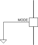
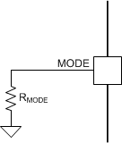
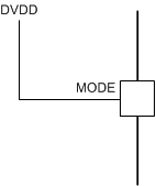
In the hardware version of the device, the MODE pin determines the control interface and latches on power-up or when exiting sleep mode. During the device power-up sequence, the DVDD pin is enabled first, and then the MODE pin latches. Tying the MODE pin directly to ground sets the mode to phase and enable. Tying the MODE pin to the DVDD pin, or an external 5 V rail, sets the mode to PWM. Connecting the MODE pin to ground with a 200 kΩ ± 5% resistor sets the mode to independent half-bridge where the two half-bridges can be independently controlled by their respective input (INx) pins. Table 7-3 lists the different MODE pin settings.

Table 7-3 DRV8873H-Q1 MODE Pin Settings
CONNECTIONMODECIRCUIT
Connect to GNDPhase and EnableGUID-928D64C2-9113-4FF1-99DD-80B1295A0AD4-low.gif
200 kΩ ± 5% to GNDIndependent half-bridgeGUID-94CCB4DB-D0CE-48BF-9CB6-10D9CFE004B4-low.gif
Connect to DVDDPWMGUID-DFC15D84-C404-4619-8EE3-A75FD82B7BA5-low.gif

In the SPI version of the device, the mode setting can be changed by writing to the MODE register in the IC1 control register because this device version has no dedicated MODE pin. The device mode gets latched when the DISABLE signal transitions from high to low.