DS100BR111A Ultra Low Power 10.3 Gbps 1-Lane Repeaters with Input Equalization and Output De-Emphasis
1 Features
- Two Channel Repeaters for up to 10.3 Gbps
- DS100BR111 : 1x Bidirectional Lane
- DS100BR210: 2x Unidirectional Channels
- DS100BR111A : 1x Bidirectional Lane
- Low 65 mW/channel (Typical) Power Consumption, with Option to Power Down Unused Channels
- Advanced Signal Conditioning Features
- Receive Equalization up to +36 dB
- Transmit De-emphasis up to -12 dB
- Transmit VOD Control: 600 to 1200 mVp-p
- Low Residual DJ at 10.3 Gbps
- Programmable Via Pin Selection, EEPROM, or SMBus Interface
- Single Supply Voltage: 2.5 V or 3.3 V
- Flow-thru Pinout in 4 mm × 4 mm 24-pin Leadless WQFN Package
- 5 kV HBM ESD Rating
- -40 to 85°C Operating Temperature Range
2 Applications
- High-speed Active Copper Cable Modules in Communication Systems
- 10GE, FC, SAS, SATA 3/6 Gbps (with OOB Detection), InfiniBand, CPRI, RXAUI and many others
3 Description
The DS100BR111A is an extremely low power, high performance repeater designed to support serial links with data rates up to 10.3 Gbps. The DS100BR111A pinout is configured as one bidirectional lane (one transmit, one receive channel). The DS100BR111A inputs feature a powerful 4-stage continuous time linear equalizer (CTLE) to provide a boost of up to +36 dB at 5 GHz and open an input eye that is completely closed due to inter-symbol interference (ISI) induced by the interconnect mediums such as board traces or twin-axial copper cables. The transmitter features a programmable output de-emphasis driver with up to -12 dB and can drive output voltage levels from 600 mVp-p to 1200 mVp-p.
The programmable settings can be applied via pin control, SMBus protocol, or an external EEPROM. In the EEPROM mode, the configuration information is automatically loaded on power up, thereby eliminating the need for an external microprocessor or software driver. The DS100BR111A consumes just 65 mW/channel (typical), and allows the option to turn off unused channels. This ultra low power consumption eliminates the need for external heat sinks and simplifies thermal management in active cable applications.
Device Information(1)
| PART NUMBER | PACKAGE | BODY SIZE (NOM) |
|---|---|---|
| DS100BR111A | WQFN (24) | 4.00 mm x 4.00 mm |
- For all available packages, see the orderable addendum at the end of the datasheet.
4 Simplified Schematic

Typical Application

5 Revision History
Changes from C Revision (April 2013) to D Revision
6 Pin Configuration and Functions
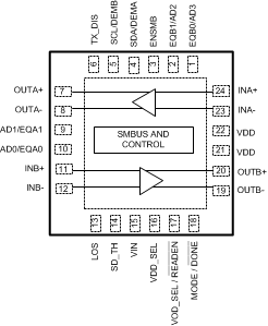
Pin Functions(1)
| PIN | I/O, TYPE | DESCRIPTION | ||
|---|---|---|---|---|
| NAME | NUMBER | |||
| DIFFERENTIAL HIGH SPEED I/O's | ||||
| INA+, INA- , INB+, INB- |
24, 23 11, 12 |
I, CML | Inverting and non-inverting CML differential inputs to the equalizer. On-chip 50 Ω termination resistors connect both INx+ and INx- to VDD. Compatible with AC coupled CML inputs. | |
| OUTA+, OUTA-, OUTB+, OUTB- |
7, 8 20, 19 |
O, CML | Inverting and non-inverting 50 Ω driver outputs with de-emphasis. Compatible with AC coupled CML inputs. | |
| CONTROL PINS | ||||
| ENSMB | 3 | I, 4-LEVEL, LVCMOS |
System Management Bus (SMBus) Enable Pin High = Register Access SMBus Slave Mode Float = Read External EEPROM (SMBus Master Mode) Tie 1 kΩ to GND = Pin Mode |
|
| ENSMB = Float or 1 (SMBus MODES) | ||||
| SCL | 5 | I, 2-LEVEL, LVCMOS, O, Open Drain |
Clock output when loading EEPROM configuration, reverting to SMBus clock input when EEPROM load is complete (ALL_DONE = 0). External 2 kΩ to 5 kΩ pull-up resistor to VDD (2.5 V mode) or VIN (3.3 V mode) recommended as per SMBus interface standards(2) |
|
| SDA | 4 | I, 2-LEVEL, LVCMOS, O, Open Drain |
In both SMBus Modes, this pin is the SMBus data I/O. Data input or open drain output. External 2 kΩ to 5 kΩ pull-up resistor to VDD (2.5 V mode) or VIN (3.3 V mode) recommended as per SMBus interface standards(2) |
|
| AD0-AD3 | 10, 9, 2, 1 | I, 4-LEVEL, LVCMOS |
ENSMB Master or Slave mode SMBus Slave Address Inputs. In SMBus mode, these pins are the user set SMBus slave address inputs. There are 16 addresses supported by these pins. Pins must be tied Low or HIGH when used to define the device SMBus address. (4) |
|
| READEN | 17 | I, 2-LEVEL, LVCMOS |
ENSMB = Float: When using SMBus Master Mode, a logic low on this pin starts the load from the external EEPROM. ENSMB = 1: When using SMBus Slave Mode, the VOD_SEL/READEN pin must be tied Low for the AD[3:0] to be active. If this pin is tied High or left floating, an address of 0xB0 will be used for the DS100BR111A. |
|
| DONE | 18 | O, 2-LEVEL, LVCMOS |
When using an External EEPROM (ENSMB = Float), Valid Register Load Status Output High = External EEPROM load failed or incomplete Low = External EEPROM load passed |
|
| ENSMB = 0 (PIN MODE) | ||||
| EQA0, EQA1 EQB0, EQB1 |
10, 9 1, 2 |
I, 4-LEVEL, LVCMOS |
EQA[1:0] and EQB[1:0] control the level of equalization on the input pins. EQA[1:0] controls the A channel, and EQB[1:0] controls the B channel. The pins are only active when ENSMB = 0. When ENSMB = 1, the SMBus registers provide independent control of each channel, and the EQB0/B1 pins are converted to SMBus AD2/AD3 inputs. See Table 3 for additional information. |
|
| DEMA, DEMB | 4, 5 | I, 4-LEVEL, LVCMOS |
DEMA and DEMB control the level of de-emphasis for the output driver when in 10G mode. DEMA controls the A channel, and DEMB controls the B channel. The pins are only active when ENSMB = 0. When ENSMB = 1, the SMBus registers provide independent control of each channel, and the DEM pins are converted to SMBus SCL and SDA pins. See Table 4 for additional information. |
|
| VOD_SEL | 17 | I, 4-LEVEL, LVCMOS |
VOD Select High = (VOD = 950 mVpp or 1150 mVpp) Float = (VOD = 850 mVpp) 20 kΩ to GND = (VOD = 1050 mVpp) 1 kΩ to GND = (VOD = 575 mVpp) See (4)(5) for additional notes. See Table 2 for additional information. |
|
| MODE | 18 | I, 4-LEVEL, LVCMOS |
Controls Device Mode of Operation High= 10GbE Mode, Continuous Talk (Output Always On) Float = Slow OOB 20 kΩ to GND = eSATA Mode, Fast OOB, Auto Low Power on 100 µs of inactivity. SD stays active. 1 kΩ to GND = SAS Mode, Fast OOB |
|
| CONTROL PINS — BOTH PIN AND SMBus MODES (LVCMOS) | ||||
| TX_DIS | 6 | I, 2-LEVEL, LVCMOS |
High = OUTA Enabled, OUTB Disabled Low = OUTA and OUTB Enabled |
|
| LOS | 13 | O, Open Drain | Indicates Loss of Signal (Default is LOS on INA). Can be modified via SMBus registers. | |
| SD_TH | 14 | I, 4-LEVEL, LVCMOS |
The SD_TH pin controls LOS threshold setting Assert (mVpp), Deassert (mVpp) High = 190 mVpp, 130 mVpp Float = 180 mVpp, 110 mVpp (Default) 20 kΩ to GND = 160 mVpp, 100 mVpp 1 kΩ to GND = 210 mVpp, 150 mVpp(3) |
|
| VDD_SEL | 16 | I, FLOAT | Enables the 3.3 V to 2.5 V internal regulator Low = 3.3 V Operation Float = 2.5 V Operation |
|
| POWER | ||||
| VDD | 21, 22 | Power | Power supply pins When in 2.5 V mode, connect to 2.5 V supply. When in 3.3 V mode, do not connect to any supply voltage. Should be used to attach external decoupling to device, 100 nF recommended. See Power Supply Recommendations for additional information. |
|
| VIN | 15 | Power | VIN = 3.3 V ± 10% (input to internal LDO regulator) When in 2.5 V mode, VIN pin must be left floating. See Power Supply Recommendations for additional information. |
|
| GND | DAP | Power | Ground pad (DAP - die attach pad). | |