-
DS125BR820 Low-Power 12.5 Gbps 8-Channel Linear Repeater
- 1 Features
- 2 Applications
- 3 Description
- 4 Revision History
- 5 Pin Configuration and Functions
- 6 Specifications
- 7 Detailed Description
- 8 Applications and Implementation
- 9 Power Supply Recommendations
- 10Layout
- 11Device and Documentation Support
- 12Mechanical, Packaging, and Orderable Information
- IMPORTANT NOTICE
DS125BR820 Low-Power 12.5 Gbps 8-Channel Linear Repeater
1 Features
- Low 70 mW/Channel (Typ) Power Consumption, with Option to Power Down Unused Channels
- Seamless Link Training Support
- Enables Host ASIC to Meet Front-Port Eye Mask Requirements over Longer Reach
- Advanced Configurable Signal Conditioning I/O
- Receive CTLE up to 10 dB at 6 GHz
- Linear Output Driver
- Variable Output Voltage Range up to 1200 mVp-p
- Programmable via Pin Selection, EEPROM, or SMBus Interface
- Single Supply Voltage: 2.5 V or 3.3 V
- −40°C to 85°C Operating Temperature Range
- Flow-Thru Layout in 10 mm × 5.5 mm 54-Pin Leadless WQFN Package
2 Applications
- Front-Port 40G-CR4/SR4/LR4 Link Extension
- Backplane 40G-KR4 Link Extension
- SAS/SATA/PCIe Link Extension
- Other Proprietary High Speed Interfaces up to 12.5 Gbps
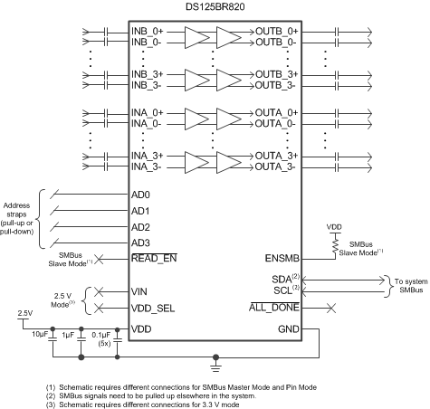
Simplified Functional Block Diagram

3 Description
The DS125BR820 is an extremely low-power high-performance repeater/redriver designed to support eight channels carrying high speed interface up to 12.5 Gbps, such as 40G-CR4, 40G-KR4, SAS/SATA, and PCIe. The receiver's continuous time linear equalizer (CTLE) provides high frequency boost that is programmable from 3 to 10 dB at 6 GHz (12 Gbps) followed by a linear output driver. The CTLE receiver is capable of opening an input eye that is completely closed due to inter symbol interference (ISI) induced by interconnect medium such as board traces or twin axial-copper cables. The programmable equalization maximizes the flexibility of physical placement within the interconnect channel and improves overall channel performance.
When operating in 40G-CR4/KR4, SAS/SATA, and PCIe applications, the DS125BR820 preserves transmit signal characteristics, thereby allowing the host controller and the end point to negotiate transmit equalizer coefficients. This transparency in the link training protocol facilitates system level interoperability and minimizes latency.
The programmable settings can be applied easily via pin control, software (SMBus or I2C), or direct loading from an external EEPROM. In EEPROM mode, the configuration information is automatically loaded on power up, thereby eliminating the need for an external microprocessor or software driver.
Device Information(1)
| PART NUMBER | PACKAGE | BODY SIZE (NOM) |
|---|---|---|
| DS125BR820 | WQFN (54) | 10 mm × 5.5 mm |
- For all available packages, see the orderable addendum at the end of the datasheet.
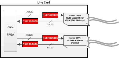
Typical Application Block Diagram

4 Revision History
Changes from A Revision (September 2014) to B Revision
- Added data type for all differential high speed I/O Go
- Changed pin assignment numbers for OUTB_2+/- and OUTB_3+/- to correct typoGo
- Changed ENSMB pin type to 4-level LVCMOS per input pin behaviorGo
- Changed Handling Ratings table to ESD Ratings table Go
- Changed register map rows to combine multiple consecutive registers with a value of all zeros and no EEPROM-relevant bitsGo
Changes from * Revision (July 2014) to A Revision
- Added release of the full document Go
5 Pin Configuration and Functions

NOTE:
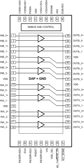
Above 54-lead WQFN graphic is a TOP VIEW, looking down through the package.Pin Functions(1)
| PIN | I/O, TYPE | PIN DESCRIPTION | |
|---|---|---|---|
| NAME | NO. | ||
| DIFFERENTIAL HIGH SPEED I/O | |||
| INB_0+, INB_0- , INB_1+, INB_1-, INB_2+, INB_2-, INB_3+, INB_3- |
1, 2 3, 4 5, 6 7, 8 |
I, CML | Inverting and non-inverting CML differential inputs to the equalizer. On-chip 50 Ω termination resistor connects INB_n+ to VDD and INB_n- to VDD depending on the state of RXDET. See Table 2. AC coupling required on high-speed I/O |
| OUTB_0+, OUTB_0-, OUTB_1+, OUTB_1-, OUTB_2+, OUTB_2-, OUTB_3+, OUTB_3- |
45, 44 43, 42 40. 39 38, 37 |
O, CML | Inverting and non-inverting 50 Ω driver outputs. Compatible with AC coupled CML inputs. AC coupling required on high-speed I/O |
| INA_0+, INA_0- , INA_1+, INA_1-, INA_2+, INA_2-, INA_3+, INA_3- |
10, 11 12, 13 15, 16 17, 18 |
I, CML | Inverting and non-inverting CML differential inputs to the equalizer. On-chip 50 Ω termination resistor connects INA_n+ to VDD and INA_n- to VDD depending on the state of RXDET. See Table 2. AC coupling required on high-speed I/O |
| OUTA_0+, OUTA_0-, OUTA_1+, OUTA_1-, OUTA_2+, OUTA_2-, OUTA_3+, OUTA_3- |
35, 34 33, 32 31, 30 29, 28 |
O, CML | Inverting and non-inverting 50 Ω driver outputs. Compatible with AC coupled CML inputs. AC coupling required on high-speed I/O |
| CONTROL PINS — SHARED (LVCMOS) | |||
| ENSMB | 48 | I, 4-LEVEL, LVCMOS |
System Management Bus (SMBus) Enable Pin Tie 1 kΩ to VDD = Register Access SMBus Slave Mode FLOAT = Read External EEPROM (SMBus Master Mode) Tie 1 kΩ to GND = Pin Mode |
| ENSMB = 1 (SMBus SLAVE MODE) | |||
| SCL | 50 | I, LVCMOS, O, OPEN Drain |
In SMBus Slave Mode, this pin is the SMBus clock I/O. Clock input or open drain output. External 2 kΩ to 5 kΩ pull-up resistor to VDD or VIN recommended as per SMBus interface standards(2) |
| SDA | 49 | I, LVCMOS, O, OPEN Drain |
In both SMBus Modes, this pin is the SMBus data I/O. Data input or open drain output. External 2 kΩ to 5 kΩ pull-up resistor to VDD or VIN recommended as per SMBus interface standards(2) |
| AD0-AD3 | 54, 53, 47, 46 | I, LVCMOS | SMBus Slave Address Inputs. In both SMBus Modes, these pins are the user set SMBus slave address inputs. External 1 kΩ pull-up or pull-down recommended. Note: In Pin Mode, AD2 must be tied via external 1 kΩ to GND. |
| RESERVED2 | 21 | I, 4-LEVEL, LVCMOS |
Reserved For applications requiring Signal Detect status register read-back: ● Leave Pin 21 floating. ● Write Reg 0x08[2] = 1 if Pin 21 is floating. Otherwise, tie Pin 21 via external 1 kΩ to GND (External 1 kΩ to VDD is also acceptable). |
| RESERVED3 | 19 | I, 4-LEVEL, LVCMOS |
Reserved This input may be left floating, tied via 1 kΩ to VDD, or tied via 1 kΩ to GND. |
| ENSMB = Float (SMBus MASTER MODE) | |||
| SCL | 50 | I, LVCMOS, O, OPEN Drain |
Clock output when loading EEPROM configuration, reverting to SMBus clock input when EEPROM load is complete (ALL_DONE = 0). External 2 kΩ to 5 kΩ pull-up resistor to VDD or VIN recommended as per SMBus interface standards(2) |
| SDA | 49 | I, LVCMOS, O, OPEN Drain |
In both SMBus Modes, this pin is the SMBus data I/O. Data input or open drain output. External 2 kΩ to 5 kΩ pull-up resistor to VDD or VIN recommended as per SMBus interface standards(2) |
| AD0-AD3 | 54, 53, 47, 46 | I, LVCMOS | SMBus Slave Address Inputs. In both SMBus Modes, these pins are the user set SMBus slave address inputs. External 1 kΩ pull-up or pull-down recommended. Note: In Pin Mode, AD2 must be tied via external 1 kΩ to GND. |
| READ_EN | 26 | I, LVCMOS | A logic low on this pin starts the load from the external EEPROM(3). Once EEPROM load is complete (ALL_DONE = 0), this pin functionality remains as READ_EN. It does not revert to an SD_TH input. |
| RESERVED2 | 21 | I, 4-LEVEL, LVCMOS |
Reserved For applications requiring Signal Detect status register read-back: ● Leave Pin 21 floating. ● Write Reg 0x08[2] = 1 if Pin 21 is floating. Otherwise, tie Pin 21 via external 1 kΩ to GND (External 1 kΩ to VDD is also acceptable). |
| RESERVED3 | 19 | I, 4-LEVEL, LVCMOS |
Reserved This input may be left floating, tied via 1 kΩ to VDD, or tied via 1 kΩ to GND. |
| ENSMB = 0 (PIN MODE) | |||
| EQA EQB |
20 46 |
I, 4-LEVEL, LVCMOS |
EQA and EQB pins control the level of equalization for the A-channels and B-channels, respectively. The pins are defined as EQA and EQB only when ENSMB is de-asserted (low). Each of the four A-channels have the same level unless controlled by the SMBus control registers. Likewise, each of the four B-channels have the same level unless controlled by the SMBus control registers. When the device operates in Slave or Master Mode, the SMBus registers independently control each lane, and the EQB pin is converted to an AD3 input. See Table 4. |
| VODB0 VODB1 |
53 54 |
I, 4-LEVEL, LVCMOS |
VODB[1:0] controls the output amplitude of the B-channels. The pins are defined as VODB[1:0] only when ENSMB is de-asserted (low). Each of the four B-channels have the same level unless controlled by the SMBus control registers. When the device operates in Slave or Master Mode, the SMBus registers provide independent control of each lane, and VODB[1:0] pins are converted to AD0, AD1 inputs. See Table 5. |
| VODA0 VODA1 |
49 50 |
I, 4-LEVEL, LVCMOS |
VODA[1:0] controls the output amplitude of the A-channels. The pins are defined as VODA[1:0] only when ENSMB is de-asserted (low). Each of the four A-channels have the same level unless controlled by the SMBus control registers. When the device operates in Slave or Master Mode, the SMBus registers provide independent control of each lane and the VODA[1:0] pins are converted to SCL and SDA. See Table 5. |
| AD2 | 47 | I, LVCMOS | Reserved in Pin Mode (ENSMB = 0) This input must be tied via external 1 kΩ to GND. |
| SD_TH | 26 | I, 4-LEVEL, LVCMOS |
Controls the internal Signal Detect Status Threshold value when in Pin Mode and SMBus Slave Mode. This pin is to be used for system debugging only. See Table 3 for more information. For final designs, input can be left floating, tied via 1 kΩ to VDD, or tied via 1 kΩ to GND. |
| RESERVED2 | 21 | I, 4-LEVEL, LVCMOS |
Reserved Tie via external 1 kΩ to GND (External 1 kΩ to VDD is also acceptable). |
| RESERVED3 | 19 | I, 4-LEVEL, LVCMOS |
Reserved This input must be tied via external 1 kΩ to GND. |
| CONTROL PINS — BOTH PIN AND SMBUS MODES (LVCMOS) | |||
| RXDET | 22 | I, 4-LEVEL, LVCMOS |
The RXDET pin controls the input enable function. Depending on the input level, a 50 Ω or >50 kΩ termination to the power rail is enabled. Pull up pin to VDD (2.5 V mode) or VIN (3.3 V mode) through 1 kΩ resistor to provide a 50 Ω termination to the power rail for normal operation. See Table 2. |
| RESERVED1 | 23 | I, 4-LEVEL, LVCMOS |
Reserved This input must be left floating. |
| VDD_SEL | 25 | I, FLOAT | Controls the internal regulator Float = 2.5 V mode Tie to GND = 3.3 V mode |
| PWDN | 52 | I, LVCMOS | Tie High = Low power - Power Down Tie to GND = Normal Operation See Table 2. |
| ALL_DONE | 27 | O, LVCMOS | Valid Register Load Status Output HIGH = External EEPROM load failed or incomplete LOW = External EEPROM load passed |
| POWER | |||
| VIN | 24 | Power | In 3.3 V mode, feed 3.3 V to VIN In 2.5 V mode, leave floating. |
| VDD | 9, 14, 36, 41, 51 | Power | Power Supply for CML and Analog Pins 2.5 V mode, connect to 2.5 V 3.3 V mode, connect 0.1 µF cap to each VDD Pin and GND See Power Supply Recommendations for proper power supply decoupling . |
| GND | DAP | Power | Ground pad (DAP - die attach pad). |
Input edge rate for LVCMOS/FLOAT inputs must be faster than 50 ns from 10–90%.
For 3.3 V mode operation, VIN pin input = 3.3 V and the logic "1" or "high" reference for the 4-level input is 3.3 V.
For 2.5 V mode operation, VDD pin output= 2.5 V and the logic "1" or "high" reference for the 4-level input is 2.5 V.