SNOSC82B August 2012 – June 2015 DS1776QML
PRODUCTION DATA.
- 1Features
- 2Description
- 3Revision History
- 4Pin Configuration and Functions
-
5Specifications
- 5.1 Absolute Maximum Ratings
- 5.2 ESD Ratings
- 5.3 Recommend Operating Conditions
- 5.4 Thermal Information
- 5.5 Quality Conformance Inspection
- 5.6 Pi Bus Transceiver DS1776 DC Parameters
- 5.7 Pi Bus Transceiver DS1776 AC Parameters: B To A Path
- 5.8 Pi Bus Transceiver DS1776 AC Parameters: A To B Path
- 5.9 Pi Bus Transceiver DS1776 AC Parameters: Setup / Hold / Pulse Width Specifications
- 5.10 Test Circuit And Waveforms
- 6Detailed Description
- 7Device and Documentation Support
- 8Mechanical, Packaging, and Orderable Information
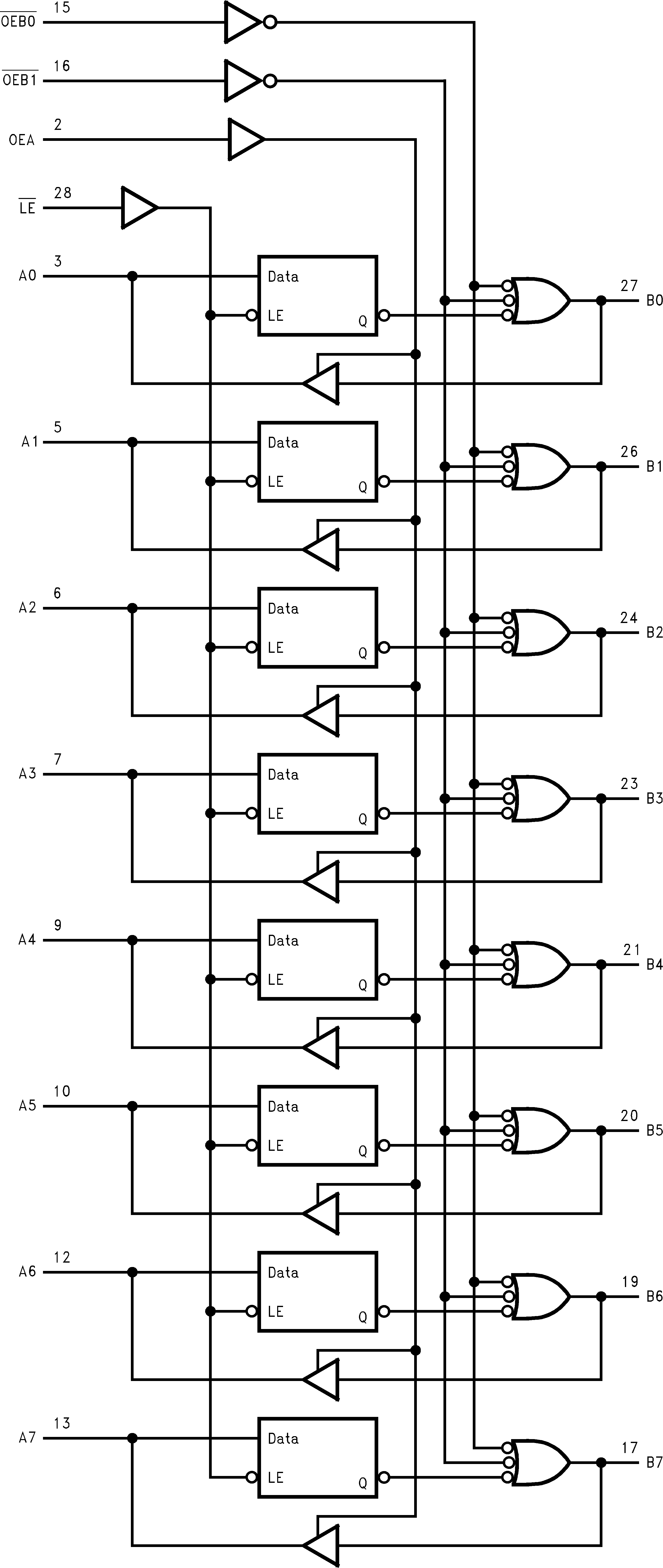
6 Detailed Description

VCC = Pin 1
VX = Pin 14
Gnd = Pins 4, 8, 11, 18, 22, 25
Figure 6. Functional Logic Diagram
VX = Pin 14
Gnd = Pins 4, 8, 11, 18, 22, 25
Table 3. Function Table(1)
| Inputs | Latch | Outputs | Mode | ||||||
|---|---|---|---|---|---|---|---|---|---|
| An | Bn(2) | LE | OEA | OEB 0 | OEB 1 | State | An | Bn | |
| H | X | L | L | L | L | H | Z | H | A TRI-STATE, Data from A to B |
| L | X | L | L | L | L | L | Z | L | |
| X | X | H | L | L | L | Qn | Z | Qn | A TRI-STATE, Latched Data to B |
| — | — | L | H | L | L | See(4) | See(2) | See(2) | Feedback: A to B, B to A |
| — | H | H | H | L | L | H(3) | H | off(3) | Preconditioned Latch Enabling |
| — | L | H | H | L | L | H(3) | L | off(3) | Data Transfer from B to A |
| — | — | H | H | L | L | Qn | Qn | Qn | Latch State to A and B |
| H | X | L | L | H | X | H | Z | off | |
| L | X | L | L | H | X | L | Z | off | B off and A TRI-STATE |
| X | X | H | L | H | X | Qn | Z | off | |
| — | H | L | H | H | X | H | H | off | |
| — | L | L | H | H | X | L | L | off | |
| — | H | H | H | H | X | Qn | H | off | B off, Data from B to A |
| — | L | H | H | H | X | Qn | L | off | |
| H | X | L | L | X | H | H | Z | off | |
| L | X | L | L | X | H | L | Z | off | B off and A TRI-STATE |
| X | X | H | L | X | H | Qn | Z | off | |
| — | H | L | H | X | H | H | H | off | |
| — | L | L | H | X | H | L | L | off | B off, Data from B to A |
| — | H | H | H | X | H | Qn | H | off | |
| — | L | H | H | X | H | Qn | L | off | |
(1) H = High Voltage Level
L = Low Voltage Level
X = Don't Care
— = Input not externally driven
Z = High Impedance (off) state
Qn = High or Low voltage level one setup time prior to the Low-to-High LE transition
L = Low Voltage Level
X = Don't Care
— = Input not externally driven
Z = High Impedance (off) state
Qn = High or Low voltage level one setup time prior to the Low-to-High LE transition
(2) Condition will cause a feedback loop path; A to B and B to A.
(3) The latch must be preconditioned such that B inputs may assume a High or Low level while OEB 0 and OEB 1, are Low and LE is high.
(4) Precaution should be taken to ensure that the B inputs do not float. If they do, they are equal to a Low state.
6.1 Controller Power Sequencing Operation
The DS1776 has a design feature which controls the output transitions during power up (or down). There are two possible conditions that occur.
- When LE = Low and OEBn = Low, the B outputs are disabled until the LE circuit can take control. This feature ensures that the B outputs will follow the A inputs and allow only one transition during power up (or down).
- If LE = High or OEBn = High, then the B outputs still remain disabled during power up (or down).