SNLS498A November 2015 – December 2015 DS90CR286AT-Q1
PRODUCTION DATA.
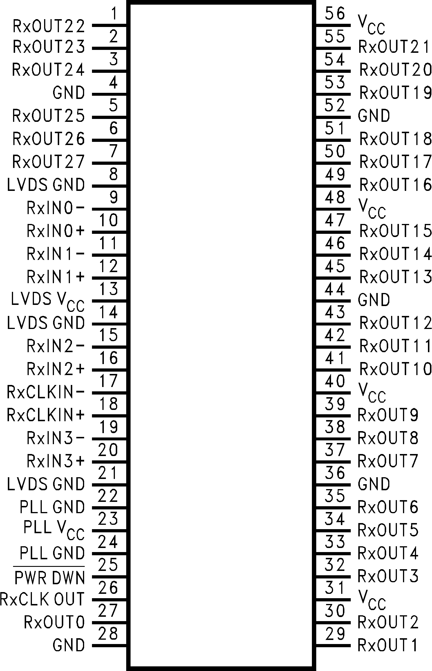
5 Pin Configuration and Functions
DGG Package
56-Pin TSSOP
Top View

Pin Functions
| PIN | I/O , TYPE | PIN DESCRIPTION | |
|---|---|---|---|
| NAME | NO. | ||
| RxIN0+, RxIN0-, RxIN1+, RxIN1-, RxIN2+, RxIN2-, RxIN3+, RxIN3- |
10, 9, 12, 11, 16, 15, 20, 19 |
I, LVDS | Positive and negative LVDS differential data inputs. 100 Ω termination resistors should be placed between RxIN+ and RxIN- receiver inputs as close as possible to the receiver pins for proper signaling. |
| RxCLKIN+, RxCLKIN- |
18, 17 |
I, LVDS | Positive and negative LVDS differential clock input. 100 Ω termination resistor should be placed between RxCLKIN+ and RxCLKIN- receiver inputs as close as possible to the receiver pins for proper signaling. |
| RxOUT[27:0] | 7, 6, 5, 3, 2, 1, 55, 54, 53, 51, 50, 49, 47, 46, 45, 43, 42, 41, 39, 38, 37, 35, 34, 33, 32, 30, 29, 27 |
O, LVCMOS | LVCMOS level data outputs. |
| RxCLK OUT | 26 | O, LVCMOS | LVCMOS Ievel clock output. The rising edge acts as the data strobe. |
| PWR DWN | 25 | I, LVCMOS | LVCMOS level input. When asserted low, the receiver outputs are low. |
| VCC | 56, 48, 40, 31 | Power | Power supply pins for LVCMOS outputs. |
| GND | 52, 44, 36, 28, 4 |
Power | Ground pins for LVCMOS outputs. |
| PLL VCC | 23 | Power | Power supply for PLL. |
| PLL GND | 24, 22 | Power | Ground pin for PLL. |
| LVDS VCC | 13 | Power | Power supply pin for LVDS inputs. |
| LVDS GND | 21, 14, 8 | Power | Ground pins for LVDS inputs. |