JAJSPJ1 December   2022 DS90LVRA2

PRODUCTION DATA  

  1. 特長
  2. アプリケーション
  3. 概要
  4. Revision History
  5. Pin Configuration and Functions
  6. Specifications
    1. 6.1 Absolute Maximum Ratings
    2. 6.2 ESD Ratings
    3. 6.3 Recommended Operating Conditions
    4. 6.4 Thermal Information
    5. 6.5 Electrical Characteristics
    6. 6.6 Switching Characteristics
    7. 6.7 Typical Characteristics
  7. Parameter Measurement Information
  8. Detailed Description
    1. 8.1 Overview
    2. 8.2 Functional Block Diagram
    3. 8.3 Feature Description
    4. 8.4 Device Functional Modes
  9. Application and Implementation
    1. 9.1 Application Information
    2. 9.2 Typical Application
      1. 9.2.1 Design Requirements
      2. 9.2.2 Detailed Design Procedure
        1. 9.2.2.1 Power Decoupling Recommendations
        2. 9.2.2.2 Termination
        3. 9.2.2.3 Input Failsafe Biasing
        4. 9.2.2.4 Probing LVDS Transmission Lines
    3. 9.3 Application Curves
  10. 10Power Supply Recommendations
  11. 11Layout
    1. 11.1 Layout Guidelines
      1. 11.1.1 Differential Traces
      2. 11.1.2 PC Board Considerations
    2. 11.2 Layout Examples
  12. 12Device and Documentation Support
    1. 12.1 Documentation Support
      1. 12.1.1 Related Documentation
    2. 12.2 ドキュメントの更新通知を受け取る方法
    3. 12.3 サポート・リソース
    4. 12.4 Trademarks
    5. 12.5 静電気放電に関する注意事項
    6. 12.6 用語集
  13. 13Mechanical, Packaging, and Orderable Information

パッケージ・オプション

メカニカル・データ(パッケージ|ピン)
サーマルパッド・メカニカル・データ
発注情報

Pin Configuration and Functions

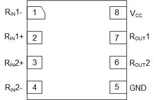
GUID-A4987E13-175B-47E7-BBC1-84A79FB7A9F7-low.gifFigure 5-1 DEM Package, WSON 8 Pin (Top View)
Table 5-1 Pin Functions
PIN TYPE(1) DESCRIPTION
NAME NO.
GND 5 G Ground pin
RIN1- 1 I Inverting receiver input pin
RIN2- 4 I
RIN1+ 2 I Non-inverting receiver input pin
RIN2+ 3 I
ROUT2 6 O Receiver output pin
ROUT1 7 O
VCC 8 P Power supply pin
I = input, O = output, G = ground