JAJSGI8D April 2016 – October 2019 DS90UB914A-Q1
PRODUCTION DATA.
- 1 特長
- 2 アプリケーション
- 3 概要
- 4 改訂履歴
- 5 概要(続き)
- 6 Device Comparison Table
- 7 Pin Configuration and Functions
-
8 Specifications
- 8.1 Absolute Maximum Ratings
- 8.2 ESD Ratings
- 8.3 Recommended Operating Conditions
- 8.4 Thermal Information
- 8.5 Electrical Characteristics
- 8.6 AC Timing Specifications (SCL, SDA) - I2C-Compatible
- 8.7 Bidirectional Control Bus DC Timing Specifications (SCL, SDA) - I2C-Compatible
- 8.8 Deserializer Switching Characteristics
- 8.9 Typical Characteristics
- 9 Parameter Measurement Information
-
10Detailed Description
- 10.1 Overview
- 10.2 Functional Block Diagram
- 10.3
Feature Description
- 10.3.1 Serial Frame Format
- 10.3.2 Line Rate Calculations for the DS90UB913A/914A
- 10.3.3 Deserializer Multiplexer Input
- 10.3.4 Error Detection
- 10.3.5 Synchronizing Multiple Cameras
- 10.3.6 General-Purpose I/O (GPIO) Descriptions
- 10.3.7 LVCMOS VDDIO Option
- 10.3.8 EMI Reduction
- 10.3.9 Pixel Clock Edge Select (TRFB / RRFB)
- 10.3.10 Power Down
- 10.4
Device Functional Modes
- 10.4.1 DS90UB913A/914A Operation With External Oscillator as Reference Clock
- 10.4.2 DS90UB913A/914A Operation With Pixel Clock From Imager as Reference Clock
- 10.4.3 MODE Pin on Deserializer
- 10.4.4 Clock-Data Recovery Status Flag (LOCK), Output Enable (OEN) and Output State Select (OSS_SEL)
- 10.4.5 Built-In Self Test
- 10.4.6 BIST Configuration and Status
- 10.4.7 Sample BIST Sequence
- 10.5 Programming
- 10.6 Register Maps
- 11Application and Implementation
- 12Power Supply Recommendations
- 13Layout
- 14デバイスおよびドキュメントのサポート
- 15メカニカル、パッケージ、および注文情報
パッケージ・オプション
メカニカル・データ(パッケージ|ピン)
- RHS|48
サーマルパッド・メカニカル・データ
- RHS|48
発注情報
10.4.1 DS90UB913A/914A Operation With External Oscillator as Reference Clock
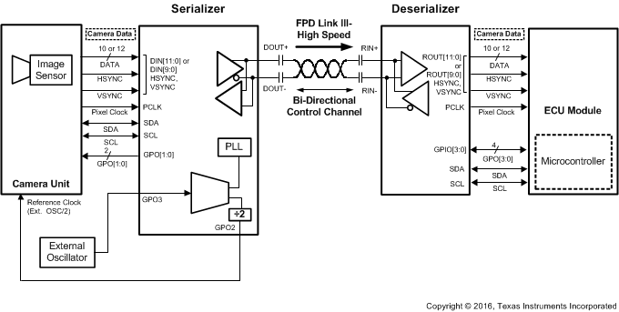
In some applications, the pixel clock that comes from the imager can have jitter which exceeds the tolerance of the DS90UB913A/914A chipsets. In this case, the DS90UB913A-Q1 device should be operated by using an external clock source as the reference clock for the DS90UB913A/914A chipsets. This is the recommended operating mode. The external oscillator clock output goes through a divide-by-2 circuit in the DS90UB913A-Q1 Serializer and this divided clock output is used as the reference clock for the imager. The output data and pixel clock from the imager are then fed into the DS90UB913A-Q1 device. Figure 16 shows the operation of the DS90UB13A/914A chipsets while using an external automotive grade oscillator.
 Figure 16. DS90UB913A-Q1/914A-Q1 Operation in the External Oscillator Mode
 When the DS90UB913A-Q1 device is operated using an external oscillator, the GPO3 pin on the DS90UB913A-Q1 is the input pin for the external oscillator. In applications where the DS90UB913A-Q1 device is operated from an external oscillator, the divide-by-2 circuit in the DS90UB913A-Q1 device feeds back the divided clock output to the imager device through GPO2 pin. The pixel clock to external oscillator ratios needs to be fixed for the 12–bit high frequency mode and the 10–bit mode. In the 10-bit mode, the pixel clock frequency divided by the external oscillator frequency must be 2. In the 12-bit high frequency mode, the pixel clock frequency divided by the external oscillator frequency must be 1.5. For example, if the external oscillator frequency is 48 MHz in the 10–bit mode, the pixel clock frequency of the imager needs to be twice of the external oscillator frequency, that is, 96 MHz. If the external oscillator frequency is 48MHz in the 12-bit high frequency mode, the pixel clock frequency of the imager needs to be 1.5 times of the external oscillator frequency, that is, 72 MHz. In external oscillator mode, GPO2 and GPO3 on the Serializer cannot act as the output of the input signal coming from GPIO2 or GPIO3 on the Deserializer.