JAJSGI8D April 2016 – October 2019 DS90UB914A-Q1
PRODUCTION DATA.
- 1 特長
- 2 アプリケーション
- 3 概要
- 4 改訂履歴
- 5 概要(続き)
- 6 Device Comparison Table
- 7 Pin Configuration and Functions
-
8 Specifications
- 8.1 Absolute Maximum Ratings
- 8.2 ESD Ratings
- 8.3 Recommended Operating Conditions
- 8.4 Thermal Information
- 8.5 Electrical Characteristics
- 8.6 AC Timing Specifications (SCL, SDA) - I2C-Compatible
- 8.7 Bidirectional Control Bus DC Timing Specifications (SCL, SDA) - I2C-Compatible
- 8.8 Deserializer Switching Characteristics
- 8.9 Typical Characteristics
- 9 Parameter Measurement Information
-
10Detailed Description
- 10.1 Overview
- 10.2 Functional Block Diagram
- 10.3
Feature Description
- 10.3.1 Serial Frame Format
- 10.3.2 Line Rate Calculations for the DS90UB913A/914A
- 10.3.3 Deserializer Multiplexer Input
- 10.3.4 Error Detection
- 10.3.5 Synchronizing Multiple Cameras
- 10.3.6 General-Purpose I/O (GPIO) Descriptions
- 10.3.7 LVCMOS VDDIO Option
- 10.3.8 EMI Reduction
- 10.3.9 Pixel Clock Edge Select (TRFB / RRFB)
- 10.3.10 Power Down
- 10.4
Device Functional Modes
- 10.4.1 DS90UB913A/914A Operation With External Oscillator as Reference Clock
- 10.4.2 DS90UB913A/914A Operation With Pixel Clock From Imager as Reference Clock
- 10.4.3 MODE Pin on Deserializer
- 10.4.4 Clock-Data Recovery Status Flag (LOCK), Output Enable (OEN) and Output State Select (OSS_SEL)
- 10.4.5 Built-In Self Test
- 10.4.6 BIST Configuration and Status
- 10.4.7 Sample BIST Sequence
- 10.5 Programming
- 10.6 Register Maps
- 11Application and Implementation
- 12Power Supply Recommendations
- 13Layout
- 14デバイスおよびドキュメントのサポート
- 15メカニカル、パッケージ、および注文情報
パッケージ・オプション
メカニカル・データ(パッケージ|ピン)
- RHS|48
サーマルパッド・メカニカル・データ
- RHS|48
発注情報
10.4.7 Sample BIST Sequence
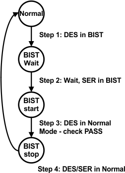
Step 1. For the DS90UB913A/914A FPD-Link III chipset, BIST Mode is enabled via the BISTEN pin of DS90UB914A-Q1 FPD-Link III deserializer. The desired clock source is selected through the deserializer GPIO0 and GPIO1 pins as shown in Table 4.
Step 2. The DS90UB913A-Q1 Serializer BIST pattern is enabled through the back channel. The BIST pattern is sent through the FPD-Link III to the deserializer. Once the serializer and deserializer are in the BIST mode and the deserializer acquires Lock, the PASS pin of the deserializer goes high and BIST starts checking FPD-Link III serial stream. If an error in the payload is detected, the PASS pin will switch low for one half of the clock period. During the BIST test, the PASS output can be monitored and counted to determine the payload error rate.
Step 3. To stop the BIST mode, the deserializer BISTEN pin is set LOW. The deserializer stops checking the data. The final test result is not maintained on the PASS pin. To monitor the BIST status, check the BIST Error Count register, 0x25 on the Deserializer.
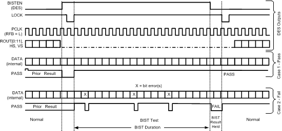
Step 4. The link returns to normal operation after the deserializer BISTEN pin is low. Figure 20 shows the waveform diagram of a typical BIST test for two cases. Case 1 is error free, and Case 2 shows one with multiple errors. In most cases, it is difficult to generate errors due to the robustness of the link (differential data transmission etc.), thus they may be introduced by greatly extending the cable length, faulting the interconnect, or by reducing signal condition enhancements (Rx equalization).
 Figure 19. AT-Speed BIST System Flow Diagram
  Figure 20. BIST Timing Diagram