JAJSGI8D April 2016 – October 2019 DS90UB914A-Q1
PRODUCTION DATA.
- 1 特長
- 2 アプリケーション
- 3 概要
- 4 改訂履歴
- 5 概要(続き)
- 6 Device Comparison Table
- 7 Pin Configuration and Functions
-
8 Specifications
- 8.1 Absolute Maximum Ratings
- 8.2 ESD Ratings
- 8.3 Recommended Operating Conditions
- 8.4 Thermal Information
- 8.5 Electrical Characteristics
- 8.6 AC Timing Specifications (SCL, SDA) - I2C-Compatible
- 8.7 Bidirectional Control Bus DC Timing Specifications (SCL, SDA) - I2C-Compatible
- 8.8 Deserializer Switching Characteristics
- 8.9 Typical Characteristics
- 9 Parameter Measurement Information
-
10Detailed Description
- 10.1 Overview
- 10.2 Functional Block Diagram
- 10.3
Feature Description
- 10.3.1 Serial Frame Format
- 10.3.2 Line Rate Calculations for the DS90UB913A/914A
- 10.3.3 Deserializer Multiplexer Input
- 10.3.4 Error Detection
- 10.3.5 Synchronizing Multiple Cameras
- 10.3.6 General-Purpose I/O (GPIO) Descriptions
- 10.3.7 LVCMOS VDDIO Option
- 10.3.8 EMI Reduction
- 10.3.9 Pixel Clock Edge Select (TRFB / RRFB)
- 10.3.10 Power Down
- 10.4
Device Functional Modes
- 10.4.1 DS90UB913A/914A Operation With External Oscillator as Reference Clock
- 10.4.2 DS90UB913A/914A Operation With Pixel Clock From Imager as Reference Clock
- 10.4.3 MODE Pin on Deserializer
- 10.4.4 Clock-Data Recovery Status Flag (LOCK), Output Enable (OEN) and Output State Select (OSS_SEL)
- 10.4.5 Built-In Self Test
- 10.4.6 BIST Configuration and Status
- 10.4.7 Sample BIST Sequence
- 10.5 Programming
- 10.6 Register Maps
- 11Application and Implementation
- 12Power Supply Recommendations
- 13Layout
- 14デバイスおよびドキュメントのサポート
- 15メカニカル、パッケージ、および注文情報
パッケージ・オプション
メカニカル・データ(パッケージ|ピン)
- RHS|48
サーマルパッド・メカニカル・データ
- RHS|48
発注情報
10.5.5 ID[x] Address Decoder on the Deserializer
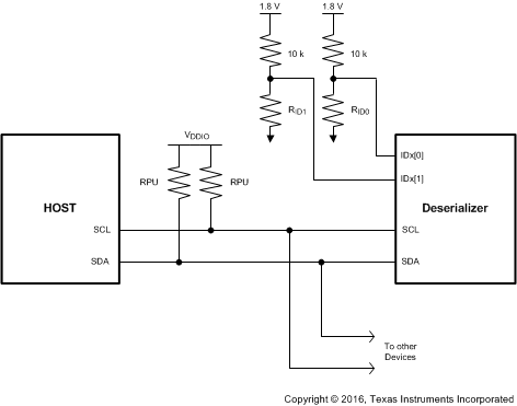
The IDx[0] and IDx[1] pins on the Deserializer are used to decode and set the physical slave address of the Deserializer (I2C only) to allow up to 16 devices on the bus using only two pins. The pins set one of 16 possible addresses for each Deserializer device. As there will be more Deserializer devices connected on the same board than Serializers, more I2C device addresses have been defined for the DS90UB914A-Q1 Deserializer than the DSDS90UB913A-Q1 Serializer. The pins must be pulled to VDD (1.8 V, not VDDIO) with a 10-kΩ resistor and two pulldown resistors (RID0 and RID1) of the recommended value to set the physical device address. The recommended maximum resistor tolerance is 1%.
 Figure 26. ID[x[ Address Decoder on the Deserializer
 Table 6. Resistor Values for IDx[0] and IDx[1] on DS90UB914A-Q1 Deserializer
| ID[x] RESISTOR VALUE — DS90UB914A-Q1 DESERIALIZER | |||
|---|---|---|---|
| RESISTOR RID1 (kΩ)
(1% TOLERANCE) |
RESISTOR RID0 (kΩ)
(1% TOLERANCE) |
ADDRESS 7'b | ADDRESS 8'b 0 APPENDED (WRITE) |
| 0 | 0 | 0x60 | 0xC0 |
| 0 | 3 | 0x61 | 0xC2 |
| 0 | 11 | 0x62 | 0xC4 |
| 0 | 100 | 0x63 | 0xC6 |
| 3 | 0 | 0x64 | 0xC8 |
| 3 | 3 | 0x65 | 0xCA |
| 3 | 11 | 0x66 | 0XCC |
| 3 | 100 | 0x67 | 0XCE |
| 11 | 0 | 0x68 | 0XD0 |
| 11 | 3 | 0x69 | 0XD2 |
| 11 | 11 | 0x6A | 0XD4 |
| 11 | 100 | 0x6B | 0XD6 |
| 100 | 0 | 0x6C | 0XD8 |
| 100 | 3 | 0x6D | 0XDA |
| 100 | 11 | 0x6E | 0XDC |
| 100 | 100 | 0x6F | 0XDE |