SNLS420D July 2012 – July 2015 DS90UB913Q-Q1 , DS90UB914Q-Q1
PRODUCTION DATA.
- 1 Features
- 2 Applications
- 3 Description
- 4 Revision History
- 5 Description continued
- 6 Device Comparison Table
- 7 Pin Configuration and Functions
-
8 Specifications
- 8.1 Absolute Maximum Ratings
- 8.2 ESD Ratings
- 8.3 Recommended Operating Conditions
- 8.4 Thermal Information
- 8.5 Electrical Characteristics
- 8.6 Timing Requirements: Recommended for Serializer PCLK
- 8.7 AC Timing Specifications (SCL, SDA) - I2C Compliant
- 8.8 Bidirectional Control Bus DC Timing Specifications (SCL, SDA) - I2C Compliant
- 8.9 Switching Characteristics: Serializer
- 8.10 Switching Characteristics: Deserializer
- 8.11 Typical Characteristics
- 9 Parameter Measurement Information
-
10Detailed Description
- 10.1 Overview
- 10.2 Functional Block Diagram
- 10.3
Feature Description
- 10.3.1 Serial Frame Format
- 10.3.2 Line Rate Calculations for the DS90UB91xQ
- 10.3.3 Deserializer Multiplexer Input
- 10.3.4 Error Detection
- 10.3.5 Description of Bidirectional Control Bus and I2C Modes
- 10.3.6 Slave Clock Stretching
- 10.3.7 I2C Pass-Through
- 10.3.8 ID[x] Address Decoder on the Serializer
- 10.3.9 ID[x] Address Decoder on the Deserializer
- 10.3.10 Programmable Controller
- 10.3.11 Synchronizing Multiple Cameras
- 10.3.12 General-Purpose I/O (GPIO) Descriptions
- 10.3.13 LVCMOS VDDIO Option
- 10.3.14 Deserializer - Adaptive Input Equalization (AEQ)
- 10.3.15 EMI Reduction
- 10.4
Device Functional Modes
- 10.4.1 DS90UB91xQ-Q1 Operation With External Oscillator as Reference Clock
- 10.4.2 DS90UB91xQ-Q1 Operation With Pixel Clock from Imager as Reference Clock
- 10.4.3 MODE Pin on Serializer
- 10.4.4 MODE Pin on Deserializer
- 10.4.5 Clock-Data Recovery Status Flag (LOCK), Output Enable (OEN) and Output State Select (OSS_SEL)
- 10.4.6 Multiple Device Addressing
- 10.4.7 Powerdown
- 10.4.8 Pixel Clock Edge Select (TRFB / RRFB)
- 10.4.9 Power-Up Requirements and PDB Pin
- 10.4.10 Built-In Self Test
- 10.4.11 BIST Configuration and Status
- 10.5 Register Maps
- 11Application and Implementation
- 12Power Supply Recommendations
- 13Layout
- 14Device and Documentation Support
- 15Mechanical, Packaging, and Orderable Information
パッケージ・オプション
デバイスごとのパッケージ図は、PDF版データシートをご参照ください。
メカニカル・データ(パッケージ|ピン)
- RHS|48
サーマルパッド・メカニカル・データ
発注情報
9 Parameter Measurement Information
9.1 AC Timing Diagrams and Test Circuits
 Figure 5. Bidirectional Control Bus Timing
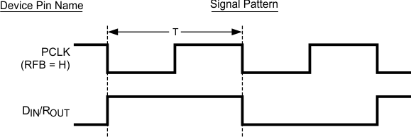 Figure 6. Worst Case Test Pattern
 Figure 7. Serializer CML Output Load and Transition Times
 Figure 8. Serializer CML Output Load and Transition Times
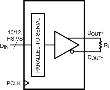 Figure 9. Serializer VOD Diagram
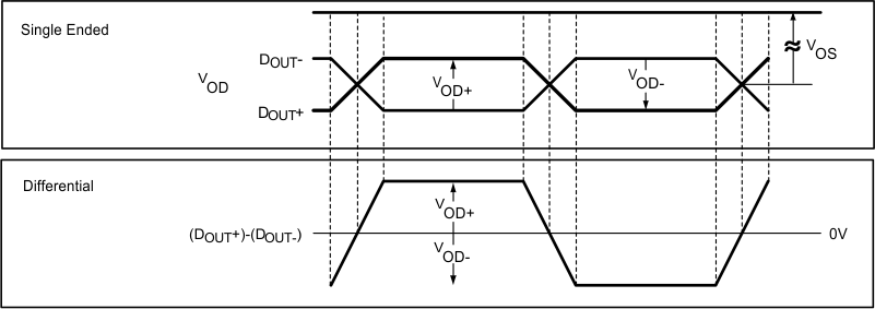 Figure 10. Serializer VOD Diagram
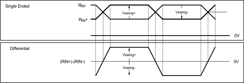 Figure 11. Differential Vswing Diagram
 Figure 12. Serializer Input Clock Transition Times
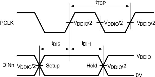 Figure 13. Serializer Set-Up and Hold Times
 Figure 14. Serializer PLL Lock Time
 Figure 15. Serializer Delay
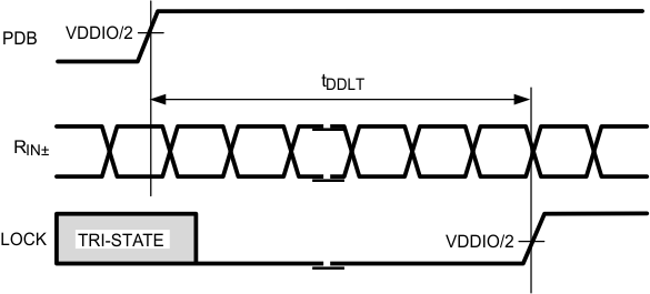 Figure 16. Deserializer Data Lock Time
 Figure 17. Deserializer LVCMOS Output Load and Transition Times
 Figure 18. Deserializer Delay
 Figure 19. Deserializer Output Set-Up and Hold Times
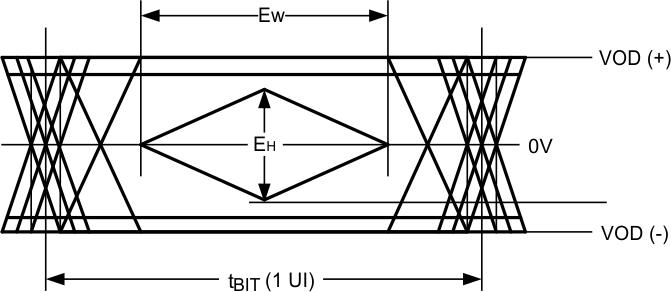 Figure 20. CML Output Driver
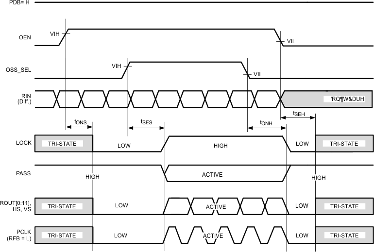 Figure 21. Output State (Set-Up and Hold) Times
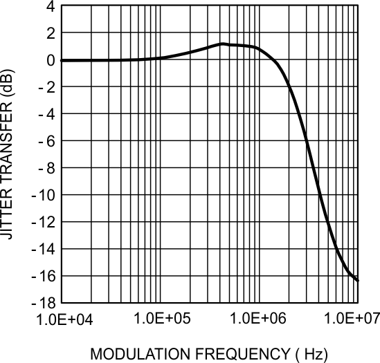 Figure 22. Typical Serializer Jitter Transfer Function at 100 MHz
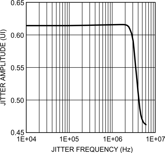 Figure 23. Typical Deserializer Input Jitter Tolerance Curve at 1.4-Gbps Line Rate
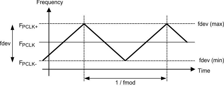 Figure 24. Spread Spectrum Clock Output Profile