SNLS512 April 2016 DS90UB924-Q1
PRODUCTION DATA.
- 1 Features
- 2 Applications
- 3 Description
- 4 Revision History
- 5 Pin Configuration and Functions
-
6 Specifications
- 6.1 Absolute Maximum Ratings
- 6.2 ESD Ratings
- 6.3 Recommended Operating Conditions
- 6.4 Thermal Information
- 6.5 DC Electrical Characteristics
- 6.6 AC Electrical Characteristics
- 6.7 DC and AC Serial Control Bus Characteristics
- 6.8 Timing Requirements for the Serial Control Bus
- 6.9 Timing Requirements
- 6.10 Typical Characteristics
-
7 Detailed Description
- 7.1 Overview
- 7.2 Functional Block Diagram
- 7.3
Feature Description
- 7.3.1 High-Speed Forward Channel Data Transfer
- 7.3.2 Low-Speed Back Channel Data Transfer
- 7.3.3 Backward Compatible Mode
- 7.3.4 Input Equalization
- 7.3.5 Common Mode Filter Pin (CMF)
- 7.3.6 Power Down (PDB)
- 7.3.7 Video Control Signals
- 7.3.8 EMI Reduction Features
- 7.3.9 Built In Self Test (BIST)
- 7.3.10 Internal Pattern Generation
- 7.3.11 Serial Link Fault Detect
- 7.3.12 Oscillator Output
- 7.3.13 Interrupt Pin (INTB / INTB_IN)
- 7.3.14 General-Purpose I/O
- 7.3.15 I2S Audio Interface
- 7.3.16 AV Mute Prevention
- 7.3.17 OEN Toggling Limitation
- 7.4 Device Functional Modes
- 7.5 Programming
- 7.6 Register Maps
- 8 Application and Implementation
- 9 Power Supply Recommendations
- 10Layout
- 11Device and Documentation Support
- 12Mechanical, Packaging, and Orderable Information
9 Power Supply Recommendations
9.1 Power Up Requirements and PDB Pin
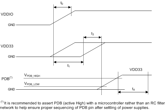
When VDDIO and VDD33 are powered separately, the VDDIO supply (1.8V or 3.3V) should ramp 100us before the other supply, VDD33. If VDDIO is tied with VDD33, both supplies may ramp at the same time. The VDDs (VDD33 and VDDIO) supply ramp should be faster than 1.5 ms with a monotonic rise. If the PDB pin is not controlled by a microcontroller, a large capacitor on the pin is needed to ensure PDB arrives after all the VDDs have settled to the recommended operating voltage. When PDB pin is pulled to VDDIO = 3.0V to 3.6V or VDD33, it is recommended to use a 10 kΩ pull-up and a >10 uF cap to GND to delay the PDB input signal.
A minimum low pulse of 2ms is required when toggling the PDB pin to perform a hard reset.
All inputs must not be driven until VDD33 and VDDIO has reached its steady state value.
 Figure 41. Power Sequence
Table 10. Power-Up Sequencing Constraints
| Symbol | Description | Test Conditions | Min | Typ | Max | Units |
|---|---|---|---|---|---|---|
| VDDIO | VDDIO voltage range | 3.0 | 3.6 | V | ||
| 1.71 | 1.89 | V | ||||
| VDD33 | VDD33 voltage range | 3.0 | 3.6 | V | ||
| VPDB_LOW | PDB LOW threshold Note: VPDB must not exceed limit for respective I/O voltage before 90% voltage of VDD33 |
VDDIO = 3.3V ± 10% | 0.8 | V | ||
| VPDB_HIGH | PDB HIGH threshold | VDDIO = 3.3V ± 10% | 2.0 | V | ||
| t0 | VDDIO rise time | These time constants are specified for rise time of power supply voltage ramp (10% - 90%) | 0.05 | 1.5 | ms | |
| t3 | VDD33 rise time | These time constants are specified for rise time of power supply voltage ramp (10% - 90%) | 0.05 | 1.5 | ms | |
| t1 | VDD33 delay time | VIL of rising edge (VDDIO ) to VIL of rising edge (VDD33) The power supplies may be ramped simultaneously. If sequenced, VDDIO must be first. |
0 | ms | ||
| t4 | Startup time | The part is powered up after the startup time has elapsed from the moment PDB goes HIGH. Local I2C is available to read/write 948/940 registers after this time. | 1 | ms |
9.2 Analog Power Signal Routing
All power inputs must be tied to the main VDD source (for example, battery), unless the user wishes to power it from another source. (that is, external LDO output).
The analog VDD inputs power the internal bias and error amplifiers, so they must be tied to the main VDD. The analog VDD inputs must have an input voltage between 2.8 V and 5.5 V, as specified in the Recommended Operating Conditions table earlier in the datasheet.
The other VINs (VINLDO1, VINLDO2) can have inputs lower than 2.8 V, as long as the input it higher than the programmed output (0.3 V).
The analog and digital grounds must be tied together outside of the chip to reduce noise coupling.