JAJSGI9D October 2014 – February 2022 DS90UB948-Q1
PRODUCTION DATA
- 1 特長
- 2 アプリケーション
- 3 概要
- 4 Revision History
- 5 Pin Configuration and Functions
-
6 Specifications
- 6.1 Absolute Maximum Ratings
- 6.2 ESD Ratings
- 6.3 Recommended Operating Conditions
- 6.4 Thermal Information
- 6.5 DC Electrical Characteristics
- 6.6 AC Electrical Characteristics
- 6.7 Timing Requirements for the Serial Control Bus
- 6.8 Switching Characteristics
- 6.9 Timing Diagrams and Test Circuits
- 6.10 Typical Characteristics
-
7 Detailed Description
- 7.1 Overview
- 7.2 Functional Block Diagram
- 7.3
Feature Description
- 7.3.1 High-Speed Forward Channel Data Transfer
- 7.3.2 Low-Speed Back Channel Data Transfer
- 7.3.3 FPD-Link III Port Register Access
- 7.3.4 Oscillator Output
- 7.3.5 Clock and Output Status
- 7.3.6 LVCMOS VDDIO Option
- 7.3.7 Power Down (PDB)
- 7.3.8 Interrupt Pin — Functional Description and Usage (INTB_IN)
- 7.3.9 General-Purpose I/O (GPIO)
- 7.3.10 SPI Communication
- 7.3.11 Backward Compatibility
- 7.3.12 Adaptive Equalizer
- 7.3.13 I2S Audio Interface
- 7.3.14 Repeater
- 7.3.15 Built-In Self Test (BIST)
- 7.3.16 Internal Pattern Generation
- 7.4
Device Functional Modes
- 7.4.1
Configuration Select MODE_SEL[1:0]
- 7.4.1.1 1-Lane FPD-Link III Input, Single Link OpenLDI Output
- 7.4.1.2 1-Lane FPD-Link III Input, Dual Link OpenLDI Output
- 7.4.1.3 2-Lane FPD-Link III Input, Dual Link OpenLDI Output
- 7.4.1.4 2-Lane FPD-Link III Input, Single Link OpenLDI Output
- 7.4.1.5 1-Lane FPD-Link III Input, Single Link OpenLDI Output (Replicate)
- 7.4.2 MODE_SEL[1:0]
- 7.4.3 OpenLDI Output Frame and Color Bit Mapping Select
- 7.4.1
Configuration Select MODE_SEL[1:0]
- 7.5 Image Enhancement Features
- 7.6
Programming
- 7.6.1 Serial Control Bus
- 7.6.2 Multi-Controller Arbitration Support
- 7.6.3 I2C Restrictions on Multi-Controller Operation
- 7.6.4 Multi-Controller Access to Device Registers for Newer FPD-Link III Devices
- 7.6.5 Multi-Controller Access to Device Registers for Older FPD-Link III Devices
- 7.6.6 Restrictions on Control Channel Direction for Multi-Controller Operation
- 7.7 Register Maps
- 8 Application and Implementation
- 9 Power Supply Recommendations
- 10Layout
- 11Device and Documentation Support
- 12Mechanical, Packaging, and Orderable Information
パッケージ・オプション
メカニカル・データ(パッケージ|ピン)
- NKD|64
サーマルパッド・メカニカル・データ
- NKD|64
発注情報
7.6.1 Serial Control Bus
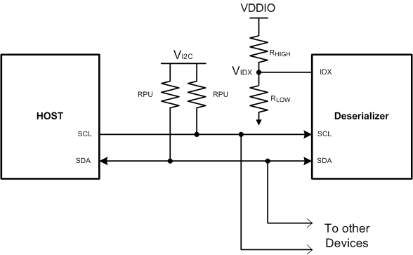
The device may also be configured by the use of a I2C-compatible serial control bus. Multiple devices may share the serial control bus (up to eight device addresses supported). The device address is set through a resistor divider (RHIGH and RLOW — see Figure 7-28 below) connected to the IDx pin.
 Figure 7-28 Serial Control Bus Connection
The serial control bus consists of two signals, SCL and SDA. SCL is a serial bus clock input. SDA is the serial bus data input / output signal. Both SCL and SDA signals require an external pullup resistor to 1.8-V or 3.3-V VI2C. For most applications, TI recommends that the user adds a 4.7-kΩ pullup resistor to the VDD33 or 2.2 kΩ resistor to the VDD18. However, the pullup resistor value may be adjusted for capacitive loading and data rate requirements. The signals are either pulled high or driven low. For more details information on how to calculate the pullup resistor, see I2C Bus Pullup Resistor Calculation (SLVA689).
The IDx pin configures the control interface to one of eight possible device addresses. A pullup resistor and a pulldown resistor may be used to set the appropriate voltage ratio between the IDx input pin (VLOW) and VDD33, each ratio corresponding to a specific device address. See Table 7-11 for more information.
| NO. | VIDX VOLTAGE | VIDX TARGET VOLTAGE | SUGGESTED STRAP RESISTORS (1% tolerance) | PRIMARY ASSIGNED I2C ADDRESS | ||
|---|---|---|---|---|---|---|
| V (TYP) | VDD = 3.3 V | R1 (kΩ) | R2 (kΩ) | 7-BIT | 8-BIT | |
| 0 | 0 | 0 | Open | 10 | 0x2C | 0x58 |
| 1 | 0.169 x V(VDD33) | 0.559 | 73.2 | 15 | 0x2E | 0x5C |
| 2 | 0.230 x V(VDD33) | 0.757 | 66.5 | 20 | 0x30 | 0x60 |
| 3 | 0.295 x V(VDD33) | 0.974 | 59 | 24.9 | 0x32 | 0x64 |
| 4 | 0.376 x V(VDD33) | 1.241 | 49.9 | 30.1 | 0x34 | 0x68 |
| 5 | 0.466 x V(VDD33) | 1.538 | 46.4 | 40.2 | 0x36 | 0x6C |
| 6 | 0.556 x V(VDD33) | 1.835 | 40.2 | 49.9 | 0x38 | 0x70 |
| 7 | 0.801 x V(VDD33) | 2.642 | 18.7 | 75 | 0x3C | 0x78 |
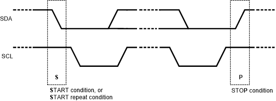
The serial bus protocol is controlled by START, START-Repeated, and STOP phases. A START occurs when SDA transitions low while SCL is high. A STOP occurs when SCL transitions high while SDA is also HIGH. See Figure 7-29.
 Figure 7-29 START and STOP Conditions
To communicate with a remote device, the host controller sends the Target address and listens for a response from the Target. This response is referred to as an acknowledge bit (ACK). If a Target on the bus is addressed correctly, it acknowledges (ACKs) the Controller by driving the SDA bus low. If the address does not match the Target address of a device, the Target not-acknowledges (NACKs) the Controller by letting the SDA be pulled High. ACKs also occur on the bus when data is transmitted. When the Controller writes data, the Target sends an ACK after every data byte is successfully received. When the Controller reads data, the Controller sends an ACK after every data byte is received to let the Target know that the Controller is ready to receive another data byte. When the Controller wants to stop reading, the Controller sends a NACK after the last data byte to create a stop condition on the bus. All communication on the bus begins with either a start condition or a repeated Start condition. All communication on the bus ends with a stop condition. A READ is shown in Figure 7-30 and a WRITE is shown in Figure 7-31.
The I2C Controller located in the deserializer must support I2C clock stretching. For more information on I2C interface requirements and throughput considerations, refer to the I2C Communication Over FPD-Link III with Bidirectional Control Channel (SNLA131).