JAJSGI9D October 2014 – February 2022 DS90UB948-Q1
PRODUCTION DATA
- 1 特長
- 2 アプリケーション
- 3 概要
- 4 Revision History
- 5 Pin Configuration and Functions
-
6 Specifications
- 6.1 Absolute Maximum Ratings
- 6.2 ESD Ratings
- 6.3 Recommended Operating Conditions
- 6.4 Thermal Information
- 6.5 DC Electrical Characteristics
- 6.6 AC Electrical Characteristics
- 6.7 Timing Requirements for the Serial Control Bus
- 6.8 Switching Characteristics
- 6.9 Timing Diagrams and Test Circuits
- 6.10 Typical Characteristics
-
7 Detailed Description
- 7.1 Overview
- 7.2 Functional Block Diagram
- 7.3
Feature Description
- 7.3.1 High-Speed Forward Channel Data Transfer
- 7.3.2 Low-Speed Back Channel Data Transfer
- 7.3.3 FPD-Link III Port Register Access
- 7.3.4 Oscillator Output
- 7.3.5 Clock and Output Status
- 7.3.6 LVCMOS VDDIO Option
- 7.3.7 Power Down (PDB)
- 7.3.8 Interrupt Pin — Functional Description and Usage (INTB_IN)
- 7.3.9 General-Purpose I/O (GPIO)
- 7.3.10 SPI Communication
- 7.3.11 Backward Compatibility
- 7.3.12 Adaptive Equalizer
- 7.3.13 I2S Audio Interface
- 7.3.14 Repeater
- 7.3.15 Built-In Self Test (BIST)
- 7.3.16 Internal Pattern Generation
- 7.4
Device Functional Modes
- 7.4.1
Configuration Select MODE_SEL[1:0]
- 7.4.1.1 1-Lane FPD-Link III Input, Single Link OpenLDI Output
- 7.4.1.2 1-Lane FPD-Link III Input, Dual Link OpenLDI Output
- 7.4.1.3 2-Lane FPD-Link III Input, Dual Link OpenLDI Output
- 7.4.1.4 2-Lane FPD-Link III Input, Single Link OpenLDI Output
- 7.4.1.5 1-Lane FPD-Link III Input, Single Link OpenLDI Output (Replicate)
- 7.4.2 MODE_SEL[1:0]
- 7.4.3 OpenLDI Output Frame and Color Bit Mapping Select
- 7.4.1
Configuration Select MODE_SEL[1:0]
- 7.5 Image Enhancement Features
- 7.6
Programming
- 7.6.1 Serial Control Bus
- 7.6.2 Multi-Controller Arbitration Support
- 7.6.3 I2C Restrictions on Multi-Controller Operation
- 7.6.4 Multi-Controller Access to Device Registers for Newer FPD-Link III Devices
- 7.6.5 Multi-Controller Access to Device Registers for Older FPD-Link III Devices
- 7.6.6 Restrictions on Control Channel Direction for Multi-Controller Operation
- 7.7 Register Maps
- 8 Application and Implementation
- 9 Power Supply Recommendations
- 10Layout
- 11Device and Documentation Support
- 12Mechanical, Packaging, and Orderable Information
パッケージ・オプション
メカニカル・データ(パッケージ|ピン)
- NKD|64
サーマルパッド・メカニカル・データ
- NKD|64
発注情報
7.3.14.1 Repeater Configuration
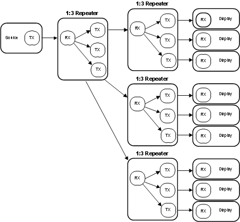
In the repeater application, this document refers to the DS90UB947-Q1 serializer or as the transmitter (TX), and refers to the DS90UB948-Q1 as the Receiver (RX). Figure 7-9 shows the maximum configuration supported for repeater implementations. Two levels of repeaters are supported with a maximum of three transmitters per receiver.
 Figure 7-9 Maximum Repeater Application
In a repeater application, the I2C interface at each TX and RX is configured to transparently pass I2C communications upstream or downstream to any I2C device within the system. This includes a mechanism for assigning alternate IDs (Target Aliases) to downstream devices in the case of duplicate addresses.