JAJSGI9D October 2014 – February 2022 DS90UB948-Q1
PRODUCTION DATA
- 1 特長
- 2 アプリケーション
- 3 概要
- 4 Revision History
- 5 Pin Configuration and Functions
-
6 Specifications
- 6.1 Absolute Maximum Ratings
- 6.2 ESD Ratings
- 6.3 Recommended Operating Conditions
- 6.4 Thermal Information
- 6.5 DC Electrical Characteristics
- 6.6 AC Electrical Characteristics
- 6.7 Timing Requirements for the Serial Control Bus
- 6.8 Switching Characteristics
- 6.9 Timing Diagrams and Test Circuits
- 6.10 Typical Characteristics
-
7 Detailed Description
- 7.1 Overview
- 7.2 Functional Block Diagram
- 7.3
Feature Description
- 7.3.1 High-Speed Forward Channel Data Transfer
- 7.3.2 Low-Speed Back Channel Data Transfer
- 7.3.3 FPD-Link III Port Register Access
- 7.3.4 Oscillator Output
- 7.3.5 Clock and Output Status
- 7.3.6 LVCMOS VDDIO Option
- 7.3.7 Power Down (PDB)
- 7.3.8 Interrupt Pin — Functional Description and Usage (INTB_IN)
- 7.3.9 General-Purpose I/O (GPIO)
- 7.3.10 SPI Communication
- 7.3.11 Backward Compatibility
- 7.3.12 Adaptive Equalizer
- 7.3.13 I2S Audio Interface
- 7.3.14 Repeater
- 7.3.15 Built-In Self Test (BIST)
- 7.3.16 Internal Pattern Generation
- 7.4
Device Functional Modes
- 7.4.1
Configuration Select MODE_SEL[1:0]
- 7.4.1.1 1-Lane FPD-Link III Input, Single Link OpenLDI Output
- 7.4.1.2 1-Lane FPD-Link III Input, Dual Link OpenLDI Output
- 7.4.1.3 2-Lane FPD-Link III Input, Dual Link OpenLDI Output
- 7.4.1.4 2-Lane FPD-Link III Input, Single Link OpenLDI Output
- 7.4.1.5 1-Lane FPD-Link III Input, Single Link OpenLDI Output (Replicate)
- 7.4.2 MODE_SEL[1:0]
- 7.4.3 OpenLDI Output Frame and Color Bit Mapping Select
- 7.4.1
Configuration Select MODE_SEL[1:0]
- 7.5 Image Enhancement Features
- 7.6
Programming
- 7.6.1 Serial Control Bus
- 7.6.2 Multi-Controller Arbitration Support
- 7.6.3 I2C Restrictions on Multi-Controller Operation
- 7.6.4 Multi-Controller Access to Device Registers for Newer FPD-Link III Devices
- 7.6.5 Multi-Controller Access to Device Registers for Older FPD-Link III Devices
- 7.6.6 Restrictions on Control Channel Direction for Multi-Controller Operation
- 7.7 Register Maps
- 8 Application and Implementation
- 9 Power Supply Recommendations
- 10Layout
- 11Device and Documentation Support
- 12Mechanical, Packaging, and Orderable Information
パッケージ・オプション
メカニカル・データ(パッケージ|ピン)
- NKD|64
サーマルパッド・メカニカル・データ
- NKD|64
発注情報
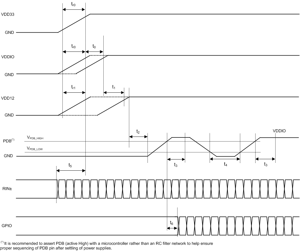
9.2 Power Sequence
 Figure 9-1 Power Sequence
Table 9-1 Power-Up Sequencing Constraints
| PARAMETER | MIN | TYP | MAX | UNIT | NOTES | |
|---|---|---|---|---|---|---|
| tr0 | VDD33 / VDDIO rise time | 0.2 | ms | @10/90% | ||
| tr1 | VDD12 rise time | 0.05 | ms | @10/90% | ||
| t0 | VDD33 to VDDIO delay | 0 | ms | |||
| t1 | VDD33 / VDDIO to VDD12 delay | 0 | ms | |||
| t2 | VDDx to PDB delay | 0 | ms | Release PDB after all supplies are up and stable. | ||
| t3 | PDB to I2C ready delay | 2 | ms | |||
| t4 | PDB pulse width | 2 | ms | Hard reset | ||
| t5 | Valid data on RIN± to VDDx delay | 0 | ms | Provide valid data from a compatible Serializer before power-up . (1) | ||
| t6 | PDB to GPIO delay | 2 | ms | Keep GPIOs low or high until PDB is high. | ||
(1) Note that the DS90UB948Q-Q1 should be powered up after a compatible Serializer has started sending valid video data. If this condition is not satisfied, then a digital (software) reset or hard reset (toggling PDB pin) is required after receiving the input data. This requirement prevents the DS90UB948Q-Q1 from locking to any random or noise signal, ensures DS90UB948Q-Q1 has a deterministic startup behavior, specified lock time, and optimal adaptive equalizer setting.