JAJSHF5 May 2019 DS90UB949A-Q1
PRODUCTION DATA.
- 1 特長
- 2 アプリケーション
- 3 概要
- 4 改訂履歴
- 5 概要(続き)
- 6 Pin Configuration and Functions
-
7 Specifications
- 7.1 Absolute Maximum Ratings
- 7.2 ESD Ratings
- 7.3 Recommended Operating Conditions
- 7.4 Thermal Information
- 7.5 DC Electrical Characteristics
- 7.6 AC Electrical Characteristics
- 7.7 DC and AC Serial Control Bus Characteristics
- 7.8 Recommended Timing for the Serial Control Bus
- 7.9 Timing Diagrams
- 7.10 Typical Characteristics
-
8 Detailed Description
- 8.1 Overview
- 8.2 Functional Block Diagram
- 8.3
Feature Description
- 8.3.1 High-Definition Multimedia Interface (HDMI)
- 8.3.2 Transition Minimized Differential Signaling
- 8.3.3 Enhanced Display Data Channel
- 8.3.4 Extended Display Identification Data (EDID)
- 8.3.5 Consumer Electronics Control (CEC)
- 8.3.6 +5-V Power Signal
- 8.3.7 Hot Plug Detect (HPD)
- 8.3.8 High-Speed Forward Channel Data Transfer
- 8.3.9 Back Channel Data Transfer
- 8.3.10 FPD-Link III Port Register Access
- 8.3.11 Power Down (PDB)
- 8.3.12 Serial Link Fault Detect
- 8.3.13 Interrupt Pin (INTB)
- 8.3.14 Remote Interrupt Pin (REM_INTB)
- 8.3.15 General-Purpose I/O
- 8.3.16 SPI Communication
- 8.3.17 Backward Compatibility
- 8.3.18 Audio Modes
- 8.3.19 Built-In Self Test (BIST)
- 8.3.20 Internal Pattern Generation
- 8.3.21 Spread-Spectrum Clock Tolerance
- 8.4 Device Functional Modes
- 8.5
Programming
- 8.5.1 Serial Control Bus
- 8.5.2 Multi-Master Arbitration Support
- 8.5.3 I2C Restrictions on Multi-Master Operation
- 8.5.4 Multi-Master Access to Device Registers for Newer FPD-Link III Devices
- 8.5.5 Multi-Master Access to Device Registers for Older FPD-Link III Devices
- 8.5.6 Restrictions on Control Channel Direction for Multi-Master Operation
- 8.5.7 Prevention of I2C Faults During Abrupt System Faults
- 8.6 Register Maps
- 9 Application and Implementation
- 10Power Supply Recommendations
- 11Layout
- 12デバイスおよびドキュメントのサポート
- 13メカニカル、パッケージ、および注文情報
10.1 Power-Up Requirements and PDB Pin
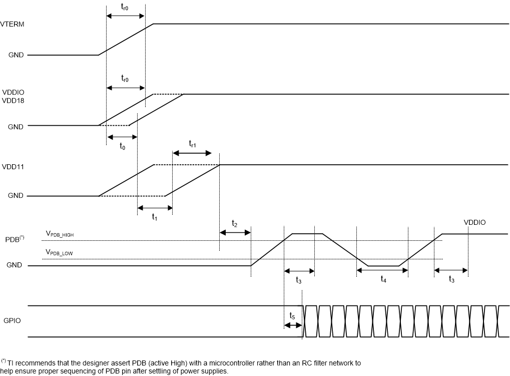
The power supply ramp should be faster than 1.5 ms with a monotonic rise. A large capacitor on the PDB pin may be used to ensure PDB arrives after all the supply pins have settled to the recommended operating voltage. When PDB pin is pulled up to VDDIO, a 10-kΩ pullup and a >10-μF capacitor to GND are required to delay the PDB input signal rise. All inputs must not be driven until all power supplies have reached steady state.
The recommended power up sequence is as follows: VDD18, VTERM, VDD11, wait until all supplies have settled, activate PDB, then apply HDMI input. There will be no functional impact to using a different sequence than shown below, but the current draw on VTERM during power up may be higher in other cases.
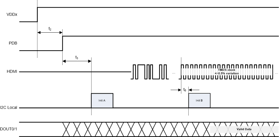
The initialization sequence A shown in Figure 33 consists of any user defined device configurations and the following:
- Set Register 0x5B bit 5 to 0. This disables the FPD3 PLL from resetting when a frequency change is detected.
- Set Register 0x16 to 0x02. This minimizes the duration of inadvertent I2C events.
The initialization sequence B shown in Figure 33 should be performed after the HDMI clock has stabilized. Sequence B consists of the following:
- Reset the HDMI PLL by writing the following registers:
- Register 0x40 = 0x10
- Register 0x41 = 0x49
- Register 0x42 = 0x10
- Register 0x42 = 0x00
- Reset the FPD PLL by writing the following registers:
- Register 0x40 = 0x14
- Register 0x41 = 0x49
- Register 0x42 = 0x10
- Register 0x42 = 0x00
 Figure 32. Recommended Power Sequencing
 VTERM must come before VDD18 when VTERM = 1.8 V. This requirement is not applicable when VTERM = 3.3 V.
 Figure 33. Initialization Sequencing
 The Init A and Init B sequence should consist of any user-defined device configurations.
Table 14. Power-Up Sequencing Constraints
| PARAMETER | TEST CONDITIONS | MIN | TYP | MAX | UNIT | |
|---|---|---|---|---|---|---|
| VDD18, VDDIO | VDD18 / VDDIO voltage range | 1.71 | 1.89 | V | ||
| VTERM | VTERM voltage range | DC-coupled HDMI termination | 3.135 | 3.465 | V | |
| AC-coupled HDMI termination | 1.71 | 1.89 | V | |||
| VDD11 | VDD11 voltage range | 1.045 | 1.155 | V | ||
| VPDB_LOW | PDB LOW threshold
Note: VPDB should not exceed limit for respective I/O voltage before 90% voltage of VDD12 |
VDDIO = 1.8V ± 5% | 0.35 × VDDIO | V | ||
| VPDB_HIGH | PDB HIGH threshold | VDDIO = 1.8V ± 5% | 0.65 × VDDIO | V | ||
| tr0 | VTERM / VDDIO / VDD18 rise time | These time constants are specified for rise time of power supply voltage ramp (10% -90%). | 1.5 | ms | ||
| tr1 | VDD11 rise time | These time constants are specified for rise time of power supply voltage ramp (10% -90%). | 1.5 | ms | ||
| t0 | VDDIO / VDD18 delay time | VTERM needs to ramp-up before VDD18 and VDDIO. | 0 | ms | ||
| t1 | VDD11 delay time | VDDIO and VDD18 need to ramp-up before VDD11. | 0 | ms | ||
| t2 | PDB delay time | PDB should be released after all supplies are stable. | 0 | ms | ||
| t3 | I2C ready time | Starting from PDB high, the local I2C access is available after this time. | 2 | ms | ||
| t4 | Hard reset time | PDB negative pulse width required for the device reset. | 2 | ms | ||
| t5 | PDB to HDMI delay time | Keep GPIOs low or high until after PDB release. | 0 | ms | ||
| t6 | HDMI Clock Stable to PLL Reset (Init B) | HDMI Clock must be within 0.5% of the target frequency and stable. | 1 | µs | ||