JAJSCC4A July 2016 – January 2024 DS90UB964-Q1
PRODUCTION DATA
- 1
- 1特長
- 2アプリケーション
- 3概要
- Pin Configuration and Functions
-
4Specifications
- 4.1 Absolute Maximum Ratings
- 4.2 ESD Ratings – JEDEC
- 4.3 ESD Ratings – IEC and ISO
- 4.4 Recommended Operating Conditions
- 4.5 Thermal Information
- 4.6 DC Electrical Characteristics
- 4.7 AC Electrical Characteristics
- 4.8 Recommended Timing for the Serial Control Bus
- 4.9 AC Electrical Characteristics
- 4.10 Typical Characteristics
-
5Detailed Description
- 5.1 Overview
- 5.2 Functional Block Diagram
- 5.3 Feature Description
- 5.4
Device Functional Modes
- 5.4.1 RAW Data Type Support and Rates
- 5.4.2 MODE Pin
- 5.4.3 REFCLK
- 5.4.4 Receiver Port Control
- 5.4.5 Input Jitter Tolerance
- 5.4.6 Adaptive Equalizer
- 5.4.7 Channel Monitor Loop-Through Output Driver
- 5.4.8 RX Port Status
- 5.4.9 GPIO Support
- 5.4.10 RAW Mode LV / FV Controls
- 5.4.11 Video Stream Forwarding
- 5.4.12 CSI-2 Protocol Layer
- 5.4.13 CSI-2 Short Packet
- 5.4.14 CSI-2 Long Packet
- 5.4.15 CSI-2 Data Identifier
- 5.4.16 Virtual Channel and Context
- 5.4.17 CSI-2 Mode Virtual Channel Mapping
- 5.4.18 CSI-2 Transmitter Frequency
- 5.4.19 CSI-2 Transmitter Status
- 5.4.20 Video Buffers
- 5.4.21 CSI-2 Line Count and Line Length
- 5.4.22 FrameSync Operation
- 5.4.23
CSI-2 Forwarding
- 5.4.23.1 Best-Effort Round Robin CSI-2 Forwarding
- 5.4.23.2 Synchronized CSI-2 Forwarding
- 5.4.23.3 Basic Synchronized CSI-2 Forwarding
- 5.4.23.4 Line-Interleaved CSI-2 Forwarding
- 5.4.23.5 Line-Concatenated CSI-2 Forwarding
- 5.4.23.6 CSI-2 Replicate Mode
- 5.4.23.7 CSI-2 Transmitter Output Control
- 5.4.23.8 Enabling and Disabling CSI-2 Transmitters
- 5.5
Programming
- 5.5.1 Serial Control Bus
- 5.5.2 Second I2C Port
- 5.5.3 I2C Target Operation
- 5.5.4 Remote Target Operation
- 5.5.5 Remote Target Addressing
- 5.5.6 Broadcast Write to Remote Devices
- 5.5.7 I2C Proxy Controller
- 5.5.8 I2C Proxy Controller Timing
- 5.5.9 Interrupt Support
- 5.5.10 Timestamp – Video Skew Detection
- 5.5.11 Pattern Generation
- 5.5.12 FPD-Link BIST Mode
- 5.6 Register Maps
- 6Application and Implementation
- 7Device and Documentation Support
- 8Revision History
- 9Mechanical, Packaging, and Orderable Information
パッケージ・オプション
メカニカル・データ(パッケージ|ピン)
- RGC|64
サーマルパッド・メカニカル・データ
- RGC|64
発注情報
4.9 AC Electrical Characteristics
Over recommended operating supply and temperature ranges unless otherwise specified.
| PARAMETER | TEST CONDITIONS | PIN OR FREQUENCY | MIN | TYP | MAX | UNIT | |
|---|---|---|---|---|---|---|---|
| HSTX DRIVER | |||||||
| HSTXDBR | Data rate | CSI0_D[3:0]P/N CSI1_D[3:0]P/N | 400 | 800 | 1600 | Mbps | |
| fCLK | DDR Clock frequency | CSI0_CLKP/N CSI1_CLKP/N | 200 | 400 | 800 | MHz | |
| ΔVCMTX(HF) | Common mode voltage variations HF | Above 450MHz | CSI0_D0P/N CSI0_D1P/N CSI0_D2P/N CSI0_D3P/N CSI0_CLKP/N CSI1_D0P/N CSI1_D1P/N CSI1_D2P/N CSI1_D3P/N CSI1_CLKP/N | 15 | mVRMS | ||
| ΔVCMTX(LF) | Common mode voltage variations LF | Between 50 and 450MHz | 25 | mVRMS | |||
| tRHS tFHS | 20% to 80% Rise and Fall HS | HS data rates ≤ 1Gbps (UI ≥ 1ns) | 0.3 | UI | |||
| HS data rates > 1Gbps (UI ≤ 1ns) but less than 1.5Gbps (UI ≥ 0.667ns) | 0.35 | UI | |||||
| Applicable when supporting maximum HS data rates ≤ 1.5Gbps. | 100 | ps | |||||
| Applicable for all HS data rates when supporting > 1.5Gbps. | 0.4 | UI | |||||
| Applicable for all HS data rates when supporting > 1.5Gbps. | 50 | ps | |||||
| SDDTX | TX differential return loss | fLPMAX | HS data rates <1.5Gbps | -18 | dB | ||
| fH | -9 | dB | |||||
| fMAX | -3 | dB | |||||
| fLPMAX | HS data rates >1.5Gbps | -18 | dB | ||||
| fH | -4.5 | dB | |||||
| fMAX | -2.5 | dB | |||||
| LPTX DRIVER | |||||||
| tRLP | Rise Time LP(1) | 15% to 85% rise time | CSI0_D0P/N CSI0_D1P/N CSI0_D2P/N CSI0_D3P/N CSI1_D0P/N CSI1_D1P/N CSI1_D2P/N CSI1_D3P/N CSI0_CLKP/N CSI1_CLKP/N | 25 | ns | ||
| tFLP | Fall Time LP (1) | 15% to 85% fall time | 25 | ns | |||
| tREOT | Rise Time Post-EoT(1) | 30%-85% rise time | 35 | ns | |||
| tLP-PULSE-TX | Pulse width of the LP exclusive-OR clock(1) | First LP exclusive-OR clock pulse after Stop state or last pulse before Stop state | 40 | ns | |||
| All other pulses | 20 | ns | |||||
| tLP-PER-TX | Period of the LP exclusive-OR clock | 90 | ns | ||||
| DV/DtSR | Slew rate (1) | CLOAD = 0 pF | 500 | mV/ns | |||
| CLOAD = 5 pF | 300 | mV/ns | |||||
| CLOAD = 20 pF | 250 | mV/ns | |||||
| CLOAD = 70 pF | 150 | mV/ns | |||||
| CLOAD = 0 to 70 pF (Falling Edge Only) | 30 | mV/ns | |||||
| CLOAD = 0 to 70 pF (Rising Edge Only) | 30 | mV/ns | |||||
| CLOAD = 0 to 70 pF (Rising Edge Only) (2)(3) | 30 - 0.075×(VO,INST - 700) | mV/ns | |||||
| CLOAD = 0 to 70 pF (Rising Edge Only) (4)(5) | 25 - 0.0625×(VO,INST - 500) | mV/ns | |||||
| CLOAD | Load capacitance(1) | 0 | 70 | pF | |||
| CSI-2 TIMING SPECIFICATIONS — DATA-CLOCK TIMING (Figure 4-6, Figure 4-7) | |||||||
| UIINST | UI instantaneous | In 1, 2, 3, or 4 Lane Configuration HS Data rate = 400 Mbps | CSI0_D0P/N CSI0_D1P/N CSI0_D2P/N CSI0_D3P/N CSI1_D0P/N CSI1_D1P/N CSI1_D2P/N CSI1_D3P/N CSI0_CLKP/N CSI1_CLKP/N | 2.5 | ns | ||
| In 1, 2, 3, or 4 Lane Configuration HS Data rate = 800 Mbps | 1.25 | ns | |||||
| In 1, 2, 3, or 4 Lane Configuration HS Data rate = 1.6Gbps | 0.625 | ns | |||||
| ΔUI | UI variation | UI ≥ 1ns (Figure 4-5) | -10% | 10% | UI | ||
| UI < 1ns (Figure 4-5) | -5% | 5% | UI | ||||
| tSKEW(TX) | Data to Clock Skew (measured
at transmitter) Skew between clock and data from ideal center | HS Data rate ≤ 1Gbps (Figure 4-5) | -0.15 | 0.15 | UIINST | ||
| 1Gbps ≤ HS Data rate ≤ 1.5Gbps (Figure 4-5) | -0.2 | 0.2 | UIINST | ||||
| tSKEW(TX) static | Static Data to Clock Skew | HS Data rate > 1.5Gbps | -0.2 | 0.2 | UIINST | ||
| tSKEW(TX) dynamic | Dynamic Data to Clock Skew | HS Data rate > 1.5Gbps | -0.15 | 0.15 | UIINST | ||
| CSI-2 TIMING SPECIFICATIONS - GLOBAL OPERATION (Figure 4-6, Figure 4-7) | |||||||
| tCLK-POST | HS exit | CSI0_D0P/N CSI0_D1P/N CSI0_D2P/N CSI0_D3P/N CSI1_D0P/N CSI1_D1P/N CSI1_D2P/N CSI1_D3P/N CSI0_CLKP/N CSI1_CLKP/N | 60 + 52×UIINST | ns | |||
| tCLK-PRE | Time HS clock shall be driver prior to any associated Data Lane beginning the transition from LP to HS mode | 8 | UIINST | ||||
| tCLK-PREPARE | Clock Lane HS Entry | 38 | 95 | ns | |||
| tCLK-SETTLE | Time interval during which the HS receiver shall ignore any Clock Lane HS transitions | 95 | 300 | ns | |||
| tCLK-TERM-EN | Time-out at Clock Lane Display Module to enable HS Termination | Time for Dn to reach VTERM-EN | 38 | ns | |||
| tCLK-TRAIL | Time that the transmitter drives the HS-0 state after the last payload clock bit of a HS transmission burst | 60 | ns | ||||
| tCLK-PREPARE + tCLK-ZERO | TCLK-PREPARE + time that the transmitter drives the HS-0 state prior to starting the Clock | 300 | ns | ||||
| tD-TERM-EN | Time for the Data Lane receiver to enable the HS line termination | Time for Dn to reach V-TERM-EN | 35 + 4×UIINST | ns | |||
| tEOT | Transmitted time interval from the start of tHS-TRAIL to the start of the LP-11 state following a HS burst | 105 + 12×UIINST | ns | ||||
| tHS-EXIT | Time that the transmitter drives LP=11 following a HS burst | 100 | ns | ||||
| tHS-PREPARE | Data Lane HS Entry | 40 + 4×UIINST | 85 + 6×UIINST | ns | |||
| tHS-PREPARE + tHS-ZERO | tHS-PREPARE + time that the transmitter drives the HS-0 state prior to transmitting the Sync sequence | 145 + 10×UIINST | ns | ||||
| tHS-SETTLE | Time interval during which the HS receiver shall ignore any Data Lane HS transitions, starting from the beginning of tHS-SETTLE | 85 + 6×UIINST | 145 + 10×UIINST | ns | |||
| tHS-SKIP | Time interval during which the HS-RX should ignore any transitions on the Data Lane, following a HS burst. The end point of the interval is defined as the beginning of the LP-11 state following the HS burst. | 40 | 55 + 4×UIINST | ns | |||
| tHS-TRAIL | Data Lane HS Exit | 60 + 4×UIINST | ns | ||||
| tLPX | Transmitted length of LP state | 50 | ns | ||||
| tWAKEUP | Recovery Time from Ultra Low Power State (ULPS) | 1 | ms | ||||
(1) CLOAD includes the low-frequency equivalent transmission line capacitance. The capacitance of TX and RX are assumed to always be <10 pF. The distributed line capacitance can be up to 50 pF for a transmission line with 2ns delay.
(2) When the output voltage is between 700 mV and 930 mV
(3) Applicable when the supported data rate ≤ 1.5Gbps
(4) When the output voltage is between 550 mV and 790 mV
(5) Applicable when the supported data rate > 1.5Gbps.
 Figure 4-1 LVCMOS Transition Times
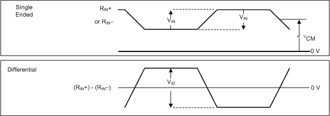 Figure 4-2 FPD-Link III Receiver VID, VIN, VCM
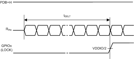 Figure 4-3 Deserializer Data Lock Time
 Figure 4-4 I2C Serial Control Bus Timing
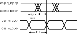 Figure 4-5 Clock and Data Timing in HS Transmission
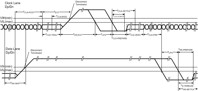 Figure 4-6 Switching the Clock Lane Between Clock
Transmission and Low-Power Mode
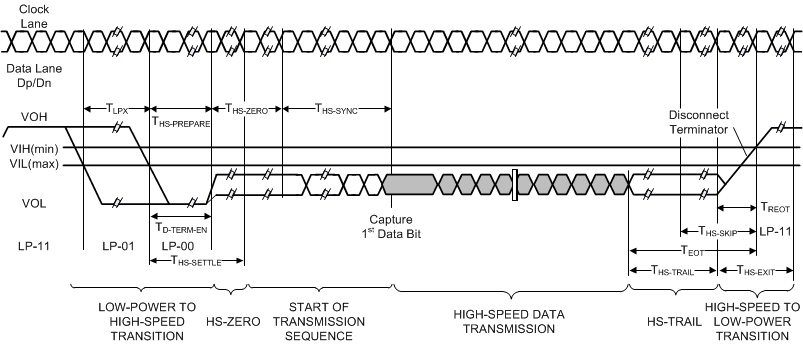 Figure 4-7 High-Speed Data Transmission Burst
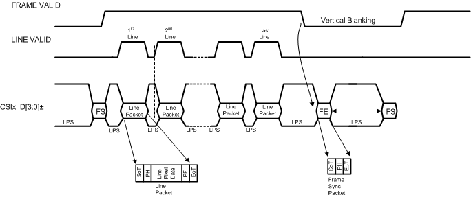 Figure 4-8 Long Line Packets and Short Frame Sync Packets
 Figure 4-9 CSI-2 General Frame Format (Single Rx / VC)
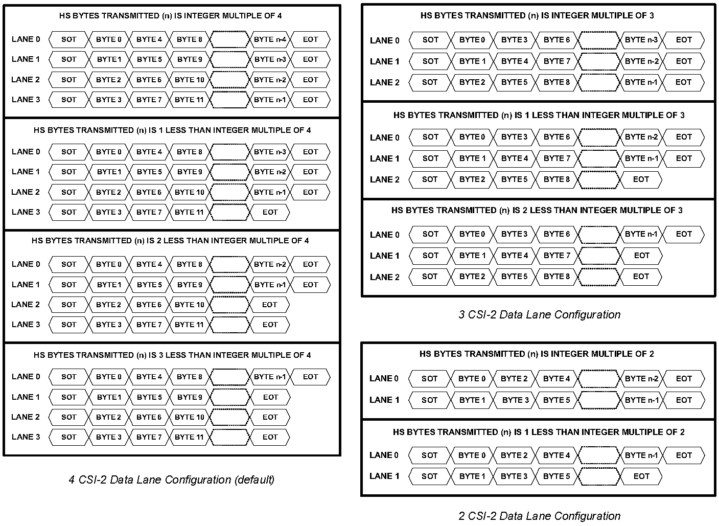 Figure 4-10 4 MIPI Data Lane Configuration