SNLS478B NOVEMBER 2014 – May 2020 DS90UH940-Q1
PRODUCTION DATA.
- 1 Features
- 2 Applications
- 3 Description
- 4 Revision History
- 5 Pin Configuration and Functions
-
6 Specifications
- 6.1 Absolute Maximum Ratings
- 6.2 ESD Ratings
- 6.3 Recommended Operating Conditions
- 6.4 Thermal Information
- 6.5 DC Electrical Characteristics
- 6.6 AC Electrical Characteristics
- 6.7 Timing Requirements for the Serial ControlBus
- 6.8 Switching Characteristics
- 6.9 Timing Diagrams and Test Circuits
- 6.10 Typical Characteristics
-
7 Detailed Description
- 7.1 Overview
- 7.2 Functional Block Diagram
- 7.3
Feature Description
- 7.3.1 High-Speed Forward Channel Data Transfer
- 7.3.2 Low-Speed Back Channel Data Transfer
- 7.3.3 FPD-Link III Port Register Access
- 7.3.4 Clock and Output Status
- 7.3.5 LVCMOS VDDIO Option
- 7.3.6 Power Down (PDB)
- 7.3.7 Interrupt Pin — Functional Description and Usage (INTB_IN)
- 7.3.8 General-Purpose I/O (GPIO)
- 7.3.9 SPI Communication
- 7.3.10 Backward Compatibility
- 7.3.11 Adaptive Equalizer
- 7.3.12 I2S Audio Interface
- 7.3.13 HDCP
- 7.3.14 Built-In Self Test (BIST)
- 7.3.15 Internal Pattern Generation
- 7.4
Device Functional Modes
- 7.4.1
Configuration Select
- 7.4.1.1 1-Lane FPD-Link III Input, 4 MIPI® Lanes Output
- 7.4.1.2 1-Lane FPD-Link III Input, 2 MIPI® Lanes Output
- 7.4.1.3 2-Lane FPD-Link III Input, 4 MIPI® Lanes Output
- 7.4.1.4 2-Lane FPD-Link III Input, 2 MIPI® Lanes Output
- 7.4.1.5 1- or 2-Lane FPD-Link III Input, 2 or 4 MIPI® Lanes Output in Replicate
- 7.4.2 MODE_SEL[1:0]
- 7.4.3 CSI-2 Interface
- 7.4.4 Input Display Timing
- 7.4.5 MIPI® CSI-2 Output Data Formats
- 7.4.6 Non-Continuous / Continuous Clock
- 7.4.7 Ultra-Low-Power State (ULPS)
- 7.4.8 CSI-2 Data Identifier
- 7.4.1
Configuration Select
- 7.5
Programming
- 7.5.1 Serial Control Bus
- 7.5.2 Multi-Master Arbitration Support
- 7.5.3 I2C Restrictions on Multi-Master Operation
- 7.5.4 Multi-Master Access to Device Registers for Newer FPD-Link III Devices
- 7.5.5 Multi-Master Access to Device Registers for Older FPD-Link III Devices
- 7.5.6 Restrictions on Control Channel Direction for Multi-Master Operation
- 7.6
Register Maps
- 7.6.1
DS90UH940-Q1 Registers
- 7.6.1.1 I2C_Device_ID Register (Address = 0h) [reset = Strap]
- 7.6.1.2 Reset Register (Address = 1h) [reset = 4h]
- 7.6.1.3 General_Configuration_0 Register (Address = 2h) [reset = 0h]
- 7.6.1.4 General_Configuration_1 Register (Address = 3h) [reset = F0h]
- 7.6.1.5 BCC_Watchdog_Control Register (Address = 4h) [reset = FEh]
- 7.6.1.6 I2C_Control_1 Register (Address = 5h) [reset = 1Eh]
- 7.6.1.7 I2C_Control_2 Register (Address = 6h) [reset = 0h]
- 7.6.1.8 REMOTE_ID Register (Address = 7h) [reset = 0h]
- 7.6.1.9 SlaveID_0 Register (Address = 8h) [reset = 0h]
- 7.6.1.10 SlaveID_1 Register (Address = 9h) [reset = 0h]
- 7.6.1.11 SlaveID_2 Register (Address = Ah) [reset = 0h]
- 7.6.1.12 SlaveID_3 Register (Address = Bh) [reset = 0h]
- 7.6.1.13 SlaveID_4 Register (Address = Ch) [reset = 0h]
- 7.6.1.14 SlaveID_5 Register (Address = Dh) [reset = 0h]
- 7.6.1.15 SlaveID_6 Register (Address = Eh) [reset = 0h]
- 7.6.1.16 SlaveID_7 Register (Address = Fh) [reset = 0h]
- 7.6.1.17 SlaveAlias_0 Register (Address = 10h) [reset = 0h]
- 7.6.1.18 SlaveAlias_1 Register (Address = 11h) [reset = 0h]
- 7.6.1.19 SlaveAlias_2 Register (Address = 12h) [reset = 0h]
- 7.6.1.20 SlaveAlias_3 Register (Address = 13h) [reset = 0h]
- 7.6.1.21 SlaveAlias_4 Register (Address = 14h) [reset = 0h]
- 7.6.1.22 SlaveAlias_5 Register (Address = 15h) [reset = 0h]
- 7.6.1.23 SlaveAlias_6 Register (Address = 16h) [reset = 0h]
- 7.6.1.24 SlaveAlias_7 Register (Address = 17h) [reset = 0h]
- 7.6.1.25 MAILBOX_18 Register (Address = 18h) [reset = 0h]
- 7.6.1.26 MAILBOX_19 Register (Address = 19h) [reset = 1h]
- 7.6.1.27 GPIO_9__Global_GPIO_Config Register (Address = 1Ah) [reset = 0h]
- 7.6.1.28 Frequency_Counter Register (Address = 1Bh) [reset = 0h]
- 7.6.1.29 General_Status Register (Address = 1Ch) [reset = 0h]
- 7.6.1.30 GPIO0_Config Register (Address = 1Dh) [reset = 0h]
- 7.6.1.31 GPIO1_2_Config Register (Address = 1Eh) [reset = 0h]
- 7.6.1.32 GPIO_3_Config Register (Address = 1Fh) [reset = 0h]
- 7.6.1.33 GPIO_5_6_Config Register (Address = 20h) [reset = 0h]
- 7.6.1.34 GPIO_7_8_Config Register (Address = 21h) [reset = 0h]
- 7.6.1.35 Datapath_Control Register (Address = 22h) [reset = 0h]
- 7.6.1.36 RX_Mode_Status Register (Address = 23h) [reset = Strap]
- 7.6.1.37 BIST_Control Register (Address = 24h) [reset = 8h]
- 7.6.1.38 BIST_ERROR_COUNT Register (Address = 25h) [reset = 0h]
- 7.6.1.39 SCL_High_Time Register (Address = 26h) [reset = 83h]
- 7.6.1.40 SCL_Low_Time Register (Address = 27h) [reset = 84h]
- 7.6.1.41 Datapath_Control_2 Register (Address = 28h) [reset = Loaded from SER]
- 7.6.1.42 I2S_Control Register (Address = 2Bh) [reset = 0h]
- 7.6.1.43 PCLK_Test_Mode Register (Address = 2Eh) [reset = 0h]
- 7.6.1.44 DUAL_RX_CTL Register (Address = 34h) [reset = 1h]
- 7.6.1.45 AEQ_CTL1 Register (Address = 35h) [reset = 0h]
- 7.6.1.46 MODE_SEL Register (Address = 37h) [reset = 0h]
- 7.6.1.47 I2S_DIVSEL Register (Address = 3Ah) [reset = 0h]
- 7.6.1.48 Adaptive_EQ_Status Register (Address = 3Bh) [reset = 0h]
- 7.6.1.49 LINK_ERROR_COUNT Register (Address = 41h) [reset = 3h]
- 7.6.1.50 HSCC_CONTROL Register (Address = 43h) [reset = 0h]
- 7.6.1.51 ADAPTIVE_EQ_BYPASS Register (Address = 44h) [reset = 60h]
- 7.6.1.52 AEQ_CTL2 Register (Address = 45h) [reset = 88h]
- 7.6.1.53 CML_OUTPUT_CTL1 Register (Address = 52h) [reset = 0h]
- 7.6.1.54 CML_OUTPUT_ENABLE Register (Address = 56h) [reset = 0h]
- 7.6.1.55 CML_OUTPUT_CTL2 Register (Address = 57h) [reset = 0h]
- 7.6.1.56 CML_OUTPUT_CTL3 Register (Address = 63h) [reset = 0h]
- 7.6.1.57 PGCTL Register (Address = 64h) [reset = 10h]
- 7.6.1.58 PGCFG Register (Address = 65h) [reset = 0h]
- 7.6.1.59 PGIA Register (Address = 66h) [reset = 0h]
- 7.6.1.60 PGID Register (Address = 67h) [reset = 0h]
- 7.6.1.61 PGDBG Register (Address = 68h) [reset = 0h]
- 7.6.1.62 PGTSTDAT Register (Address = 69h) [reset = 0h]
- 7.6.1.63 CSICFG0 Register (Address = 6Ah) [reset = 0h]
- 7.6.1.64 CSICFG1 Register (Address = 6Bh) [reset = 0h]
- 7.6.1.65 CSIIA Register (Address = 6Ch) [reset = 0h]
- 7.6.1.66 CSIID Register (Address = 6Dh) [reset = 0h]
- 7.6.1.67 GPIO_Pin_Status_1 Register (Address = 6Eh) [reset = 0h]
- 7.6.1.68 GPIO_Pin_Status_2 Register (Address = 6Fh) [reset = 0h]
- 7.6.1.69 RX_BKSV0 Register (Address = 80h) [reset = 0h]
- 7.6.1.70 RX_BKSV1 Register (Address = 81h) [reset = 0h]
- 7.6.1.71 RX_BKSV2 Register (Address = 82h) [reset = 0h]
- 7.6.1.72 RX_BKSV3 Register (Address = 83h) [reset = 0h]
- 7.6.1.73 RX_BKSV4 Register (Address = 84h) [reset = 0h]
- 7.6.1.74 TX_KSV0 Register (Address = 90h) [reset = 0h]
- 7.6.1.75 TX_KSV1 Register (Address = 91h) [reset = 0h]
- 7.6.1.76 TX_KSV2 Register (Address = 92h) [reset = 0h]
- 7.6.1.77 TX_KSV3 Register (Address = 93h) [reset = 0h]
- 7.6.1.78 TX_KSV4 Register (Address = 94h) [reset = 0h]
- 7.6.1.79 HDCP_DBG Register (Address = C0h) [reset = 0h]
- 7.6.1.80 HDCP_DBG2 Register (Address = C1h) [reset = 0h]
- 7.6.1.81 HDCP_STS Register (Address = C4h) [reset = 0h]
- 7.6.1.82 KSV_FIFO_DATA Register (Address = C9h) [reset = 0h]
- 7.6.1.83 KSV_FIFO_ADDR0 Register (Address = CAh) [reset = 0h]
- 7.6.1.84 KSV_FIFO_ADDR1 Register (Address = CBh) [reset = 0h]
- 7.6.1.85 RPTR_TX0 Register (Address = E0h) [reset = 0h]
- 7.6.1.86 RPTR_TX1 Register (Address = E1h) [reset = 0h]
- 7.6.1.87 RPTR_TX2 Register (Address = E2h) [reset = 0h]
- 7.6.1.88 RPTR_TX3 Register (Address = E3h) [reset = 0h]
- 7.6.1.89 HDCP_RX_ID0 Register (Address = F0h) [reset = 5Fh]
- 7.6.1.90 HDCP_RX_ID1 Register (Address = F1h) [reset = 55h]
- 7.6.1.91 HDCP_RX_ID2 Register (Address = F2h) [reset = 48h]
- 7.6.1.92 HDCP_RX_ID3 Register (Address = F3h) [reset = 39h]
- 7.6.1.93 HDCP_RX_ID4 Register (Address = F4h) [reset = 34h]
- 7.6.1.94 HDCP_RX_ID5 Register (Address = F5h) [reset = 30h]
- 7.6.2
CSI-2 Indirect Registers
- 7.6.2.1 CSI_TCK_TRAIL Register (Address = 2h) [reset = 0h]
- 7.6.2.2 RAW_ALIGN Register (Address = 9h) [reset = 0h]
- 7.6.2.3 CSI_EN_PORT0 Register (Address = 13h) [reset = 3Fh]
- 7.6.2.4 CSI_EN_PORT1 Register (Address = 14h) [reset = 0h]
- 7.6.2.5 CSIPASS Register (Address = 16h) [reset = 2h]
- 7.6.2.6 CSI_VC_ID Register (Address = 2Eh) [reset = 0h]
- 7.6.1
DS90UH940-Q1 Registers
- 8 Application and Implementation
- 9 Power Supply Recommendations
- 10Layout
- 11Device and Documentation Support
- 12Mechanical, Packaging, and Orderable Information
パッケージ・オプション
メカニカル・データ(パッケージ|ピン)
- NKD|64
サーマルパッド・メカニカル・データ
- NKD|64
発注情報
6.9 Timing Diagrams and Test Circuits
 Figure 1. Checkerboard Data Pattern
 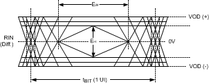 Figure 2. CML Output Driver
  Figure 3. LVCMOS Transition Times
  Figure 4. PLL Lock Time
  Figure 5. FPD-Link III Receiver DC VTH/VTL Definition
  Figure 6. Output Data Valid (Setup and Hold) Times
  Figure 7. BIST PASS Waveform
  Figure 8. Serial Control Bus Timing Diagram
 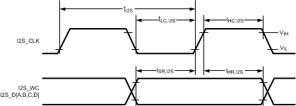 Figure 9. I2S Timing
 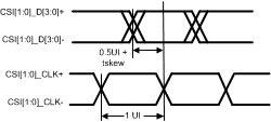 Figure 10. Clock and Data Timing in HS Transmission
 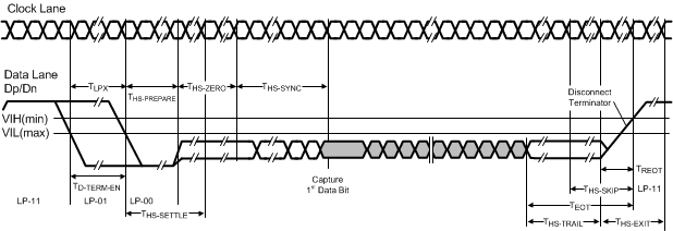 Figure 11. High-Speed Data Transmission Burst
 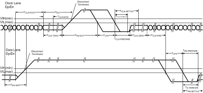 Figure 12. Switching the Clock Lane Between Clock Transmission and Low-Power Mode
 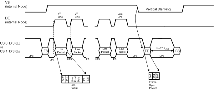 Figure 13. Long Line Packets and Short Frame Sync Packets
 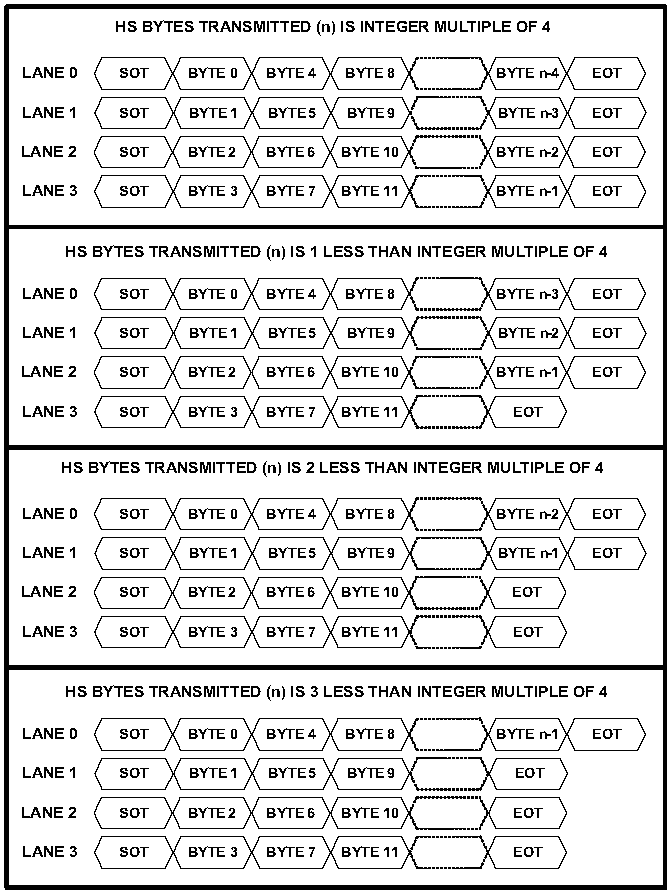 Figure 14. 4 MIPI® Data Lane Configuration
 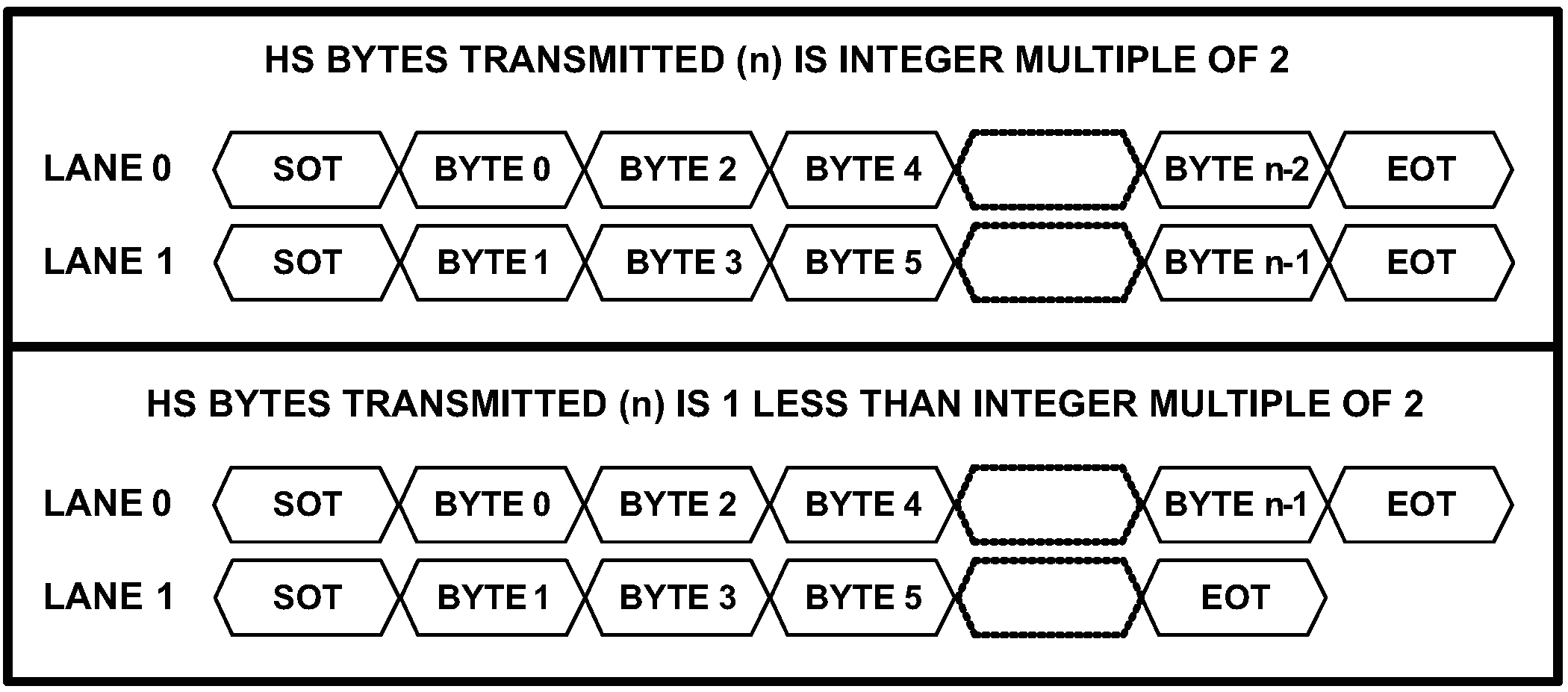 Figure 15. 2 MIPI® Data Lane Configuration