SNLS455A November 2014 – March 2019 DS90UH947-Q1
PRODUCTION DATA.
- 1 Features
- 2 Applications
- 3 Description
- 4 Revision History
- 5 Pin Configuration and Functions
-
6 Specifications
- 6.1 Absolute Maximum Ratings
- 6.2 ESD Ratings
- 6.3 Recommended Operating Conditions
- 6.4 Thermal Information
- 6.5 DC Electrical Characteristics
- 6.6 AC Electrical Characteristics
- 6.7 DC and AC Serial Control Bus Characteristics
- 6.8 Recommended Timing for the Serial Control Bus
- 6.9 Timing Diagrams
- 6.10 Typical Characteristics
-
7 Detailed Description
- 7.1 Overview
- 7.2 Functional Block Diagram
- 7.3
Feature Description
- 7.3.1 High-Speed Forward Channel Data Transfer
- 7.3.2 Back Channel Data Transfer
- 7.3.3 FPD-Link III Port Register Access
- 7.3.4 OpenLDI Input Frame and Color Bit Mapping Select
- 7.3.5 Video Control Signals
- 7.3.6 Power Down (PDB)
- 7.3.7 Serial Link Fault Detect
- 7.3.8 Interrupt Pin (INTB)
- 7.3.9 Remote Interrupt Pin (REM_INTB)
- 7.3.10 General-Purpose I/O
- 7.3.11 SPI Communication
- 7.3.12 Backward Compatibility
- 7.3.13 Audio Modes
- 7.3.14 HDCP Repeater
- 7.3.15 Built-In Self Test (BIST)
- 7.3.16 Internal Pattern Generation
- 7.4 Device Functional Modes
- 7.5
Programming
- 7.5.1 Serial Control Bus
- 7.5.2 Multi-Master Arbitration Support
- 7.5.3 I2C Restrictions on Multi-Master Operation
- 7.5.4 Multi-Master Access to Device Registers for Newer FPD-Link III Devices
- 7.5.5 Multi-Master Access to Device Registers for Older FPD-Link III Devices
- 7.5.6 Restrictions on Control Channel Direction for Multi-Master Operation
- 7.6 Register Maps
- 8 Application and Implementation
- 9 Power Supply Recommendations
- 10Layout
- 11Device and Documentation Support
- 12Mechanical, Packaging and Orderable Information
パッケージ・オプション
メカニカル・データ(パッケージ|ピン)
- RGC|64
サーマルパッド・メカニカル・データ
- RGC|64
発注情報
7.5.1 Serial Control Bus
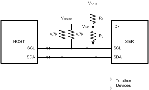
This serializer may also be configured by the use of a I2C compatible serial control bus. Multiple devices may share the serial control bus (up to 8 device addresses supported). The device address is set via a resistor divider (R1 and R2 — see Figure 31 below) connected to the IDx pin.
 Figure 31. Serial Control Bus Connection
 The serial control bus consists of two signals, SCL and SDA. SCL is a Serial Bus Clock Input. SDA is the Serial Bus Data Input / Output signal. Both SCL and SDA signals require an external pull-up resistor to VDD18 or VDD33. For most applications, a 4.7-kΩ pull-up resistor is recommended. However, the pull-up resistor value may be adjusted for capacitive loading and data rate requirements. The signals are either pulled High, or driven Low.
The IDx pin configures the control interface to one of 8 possible device addresses. A pull-up resistor and a pull-down resistor may be used to set the appropriate voltage on the IDx input pin See Table 10 below.
Table 9. Serial Control Bus Addresses For IDx
| # | RATIO
VR2 / VDD18 |
IDEAL VR2
(V) |
SUGGESTED RESISTOR R1 kΩ (1% tol) | SUGGESTED RESISTOR R2 kΩ (1% tol) | 7-BIT ADDRESS | 8-BIT ADDRESS |
|---|---|---|---|---|---|---|
| 1 | 0 | 0 | Any value less than 100 | 40.2 | 0x0C | 0x18 |
| 2 | 0.212 | 0.381 | 133 | 35.7 | 0x0E | 0x1C |
| 3 | 0.327 | 0.589 | 147 | 71.5 | 0x10 | 0x20 |
| 4 | 0.442 | 0.795 | 115 | 90.9 | 0x12 | 0x24 |
| 5 | 0.557 | 1.002 | 90.9 | 115 | 0x14 | 0x28 |
| 6 | 0.673 | 1.212 | 66.5 | 137 | 0x16 | 0x2C |
| 7 | 0.789 | 1.421 | 21.5 | 80.6 | 0x18 | 0x30 |
| 8 | 1 | 1.8 | Any value less than 100 | OPEN | 0x1A | 0x34 |
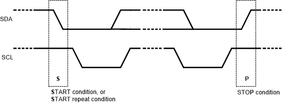
The Serial Bus protocol is controlled by START, START-Repeated, and STOP phases. A START occurs when SCL transitions Low while SDA is High. A STOP occurs when SDA transitions High while SCL is also HIGH. See Figure 32
 Figure 32. Start And Stop Conditions
 To communicate with an I2C slave, the host controller (master) sends the slave address and listens for a response from the slave. This response is referred to as an acknowledge bit (ACK). If a slave on the bus is addressed correctly, it Acknowledges (ACKs) the master by driving the SDA bus low. If the address doesn't match a device's slave address, it Not-acknowledges (NACKs) the master by letting SDA be pulled High. ACKs also occur on the bus when data is being transmitted. When the master is writing data, the slave ACKs after every data byte is successfully received. When the master is reading data, the master ACKs after every data byte is received to let the slave know it wants to receive another data byte. When the master wants to stop reading, it NACKs after the last data byte and creates a stop condition on the bus. All communication on the bus begins with either a Start condition or a Repeated Start condition. All communication on the bus ends with a Stop condition. A READ is shown in Figure 25 and a WRITE is shown in Figure 26.
 Figure 33. Serial Control Bus — Read
  Figure 34. Serial Control Bus — Write
 The I2C Master located at the serializer must support I2C clock stretching. For more information on I2C interface requirements and throughput considerations, refer to the I2C Communication Over FPD-Link III with Bidirectional Control Channel application note (SNLA131).