JAJSFV3A July   2018  – December 2018 DSLVDS1001

PRODUCTION DATA.  

  1. 特長
  2. アプリケーション
  3. 概要
    1.     機能図
    2.     代表的なアプリケーション
  4. 改訂履歴
  5. Pin Configuration and Functions
    1.     Pin Functions
  6. Specifications
    1. 6.1 Absolute Maximum Ratings
    2. 6.2 ESD Ratings
    3. 6.3 Recommended Operating Conditions
    4. 6.4 Thermal Information
    5. 6.5 Electrical Characteristics
    6. 6.6 Switching Characteristics
    7. 6.7 Typical Characteristics
  7. Parameter Measurement Information
  8. Detailed Description
    1. 8.1 Overview
    2. 8.2 Functional Block Diagram
    3. 8.3 Feature Description
      1. 8.3.1 DSLVDS1001 Driver Functionality
      2. 8.3.2 Driver Output Voltage and Power-On Reset
      3. 8.3.3 Driver Offset
    4. 8.4 Device Functional Modes
  9. Application and Implementation
    1. 9.1 Application Information
    2. 9.2 Typical Application
      1. 9.2.1 Point-to-Point Communications
    3. 9.3 Design Requirements
    4. 9.4 Detailed Design Procedure
      1. 9.4.1 Driver Supply Voltage
      2. 9.4.2 Driver Bypass Capacitance
      3. 9.4.3 Driver Input Voltage
      4. 9.4.4 Driver Output Voltage
      5. 9.4.5 Interconnecting Media
      6. 9.4.6 PCB Transmission Lines
      7. 9.4.7 Termination Resistor
    5. 9.5 Application Curve
  10. 10Power Supply Recommendations
    1. 10.1 Power Supply Considerations
  11. 11Layout
    1. 11.1 Layout Guidelines
      1. 11.1.1 Microstrip vs. Stripline Topologies
      2. 11.1.2 Dielectric Type and Board Construction
      3. 11.1.3 Recommended Stack Layout
      4. 11.1.4 Separation Between Traces
      5. 11.1.5 Crosstalk and Ground Bounce Minimization
      6. 11.1.6 Decoupling
    2. 11.2 Layout Example
  12. 12デバイスおよびドキュメントのサポート
    1. 12.1 ドキュメントのサポート
      1. 12.1.1 関連資料
    2. 12.2 ドキュメントの更新通知を受け取る方法
    3. 12.3 コミュニティ・リソース
    4. 12.4 商標
    5. 12.5 静電気放電に関する注意事項
    6. 12.6 Glossary
  13. 13メカニカル、パッケージ、および注文情報

パッケージ・オプション

メカニカル・データ(パッケージ|ピン)
サーマルパッド・メカニカル・データ
発注情報

Typical Characteristics

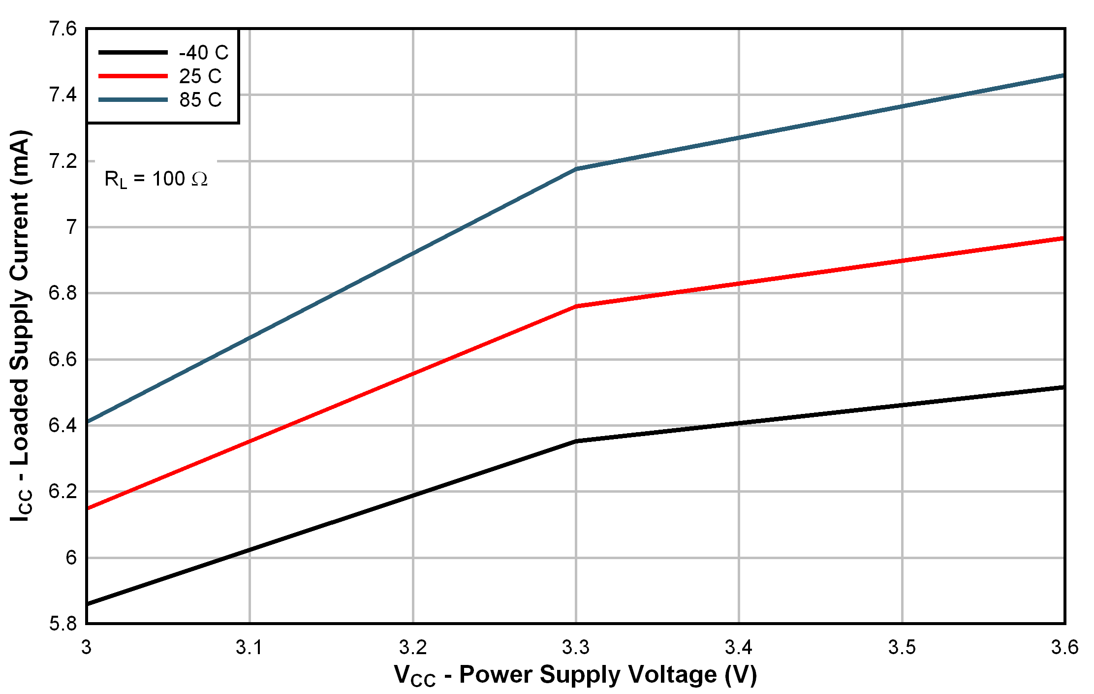
DSLVDS1001 ICC_100ohmLOAD.pngFigure 1. Loaded Supply Current vs Power Supply Voltage
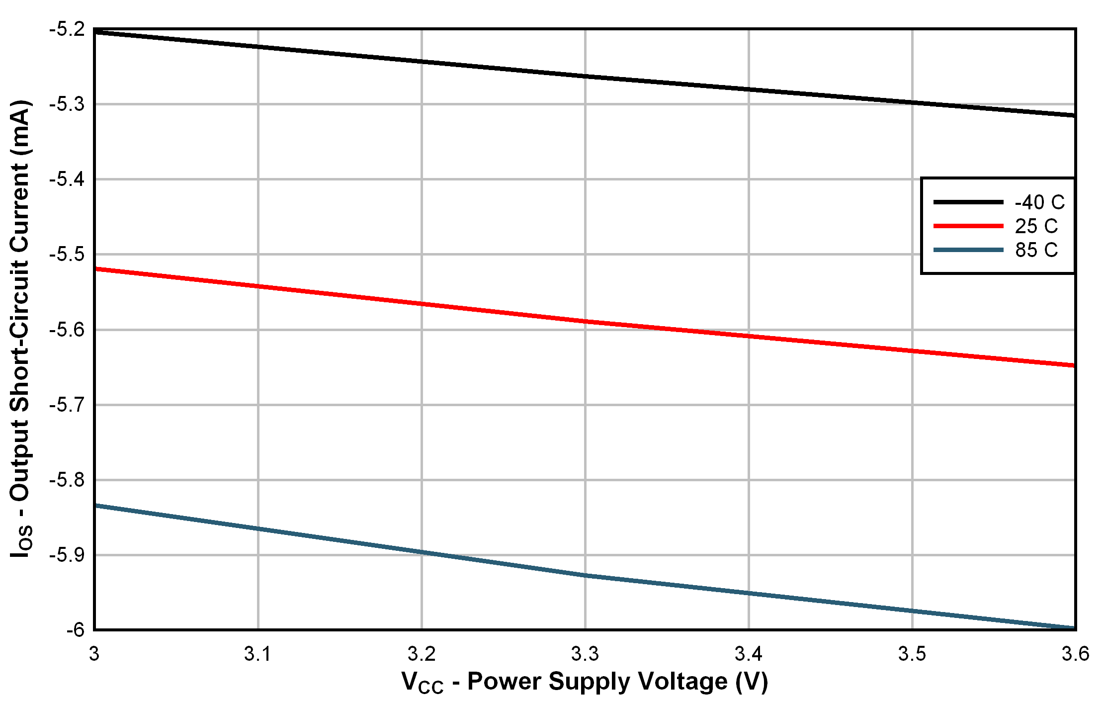
DSLVDS1001 IOS.pngFigure 3. Output Short-Circuit Current vs Power Supply Voltage
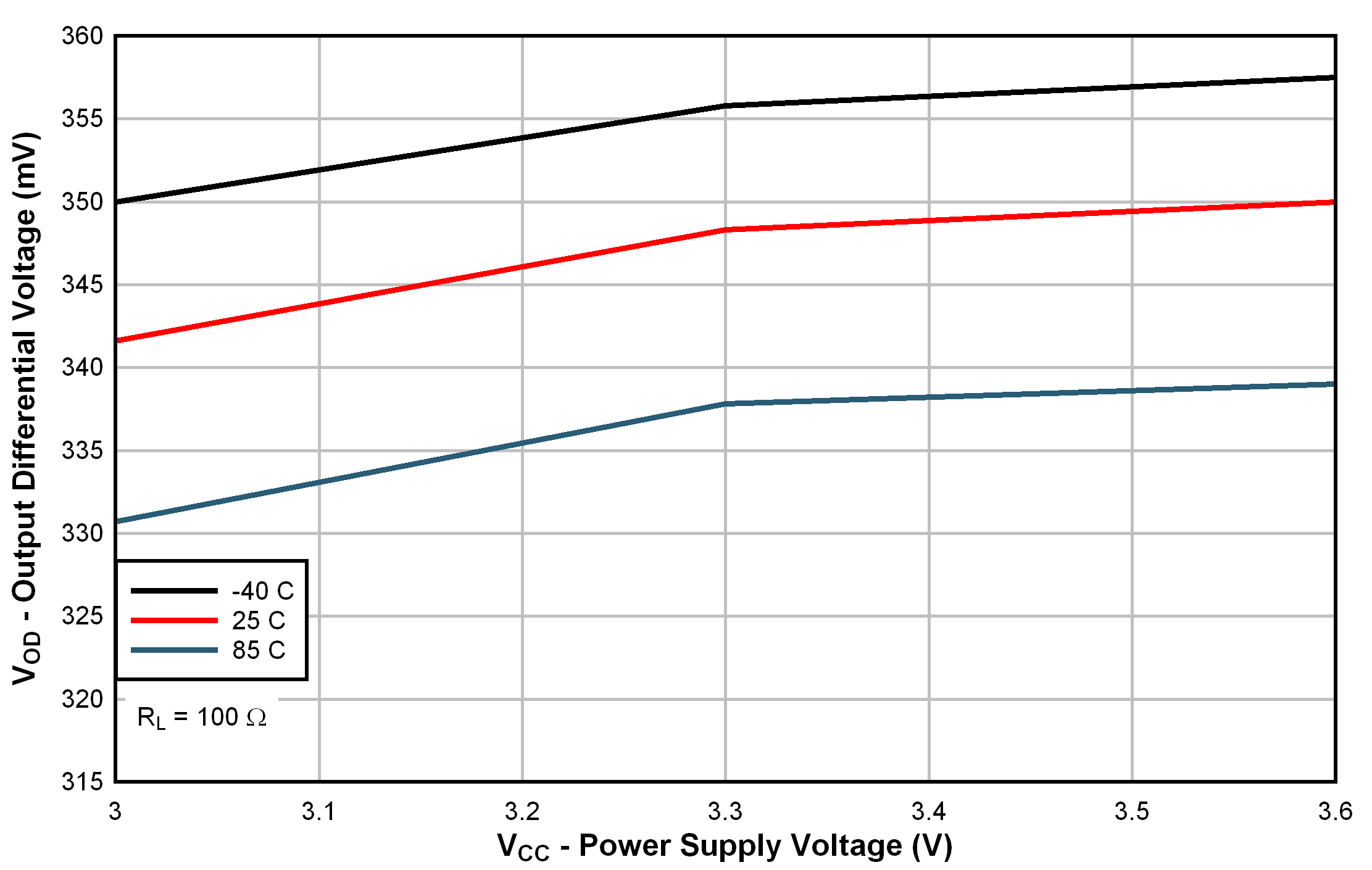
DSLVDS1001 VOD_100OhmLoad.pngFigure 5. Output Differential Voltage vs Power Supply Voltage
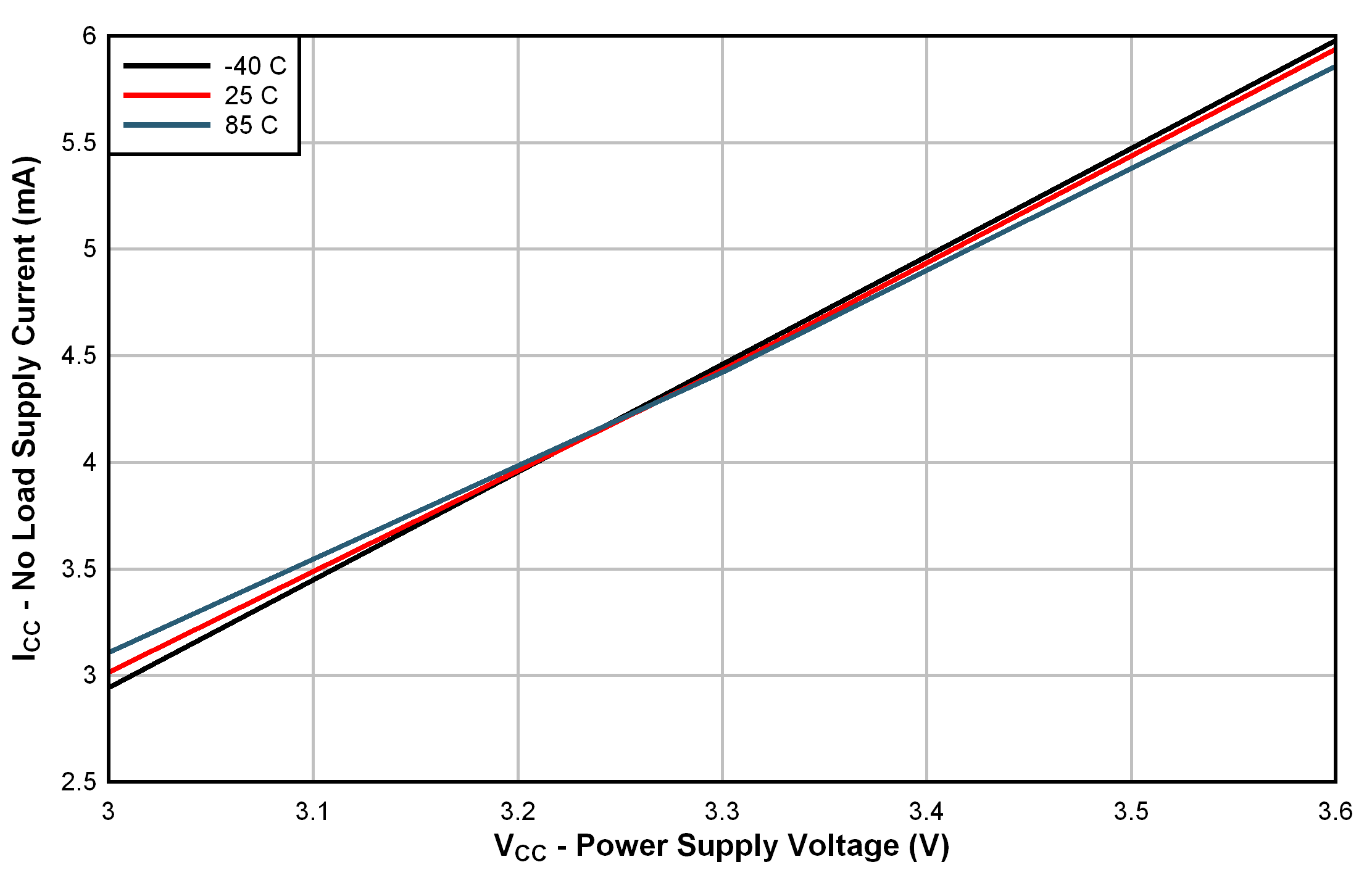
DSLVDS1001 ICC_NOLOAD.pngFigure 2. No Load Supply Current vs Power Supply Voltage
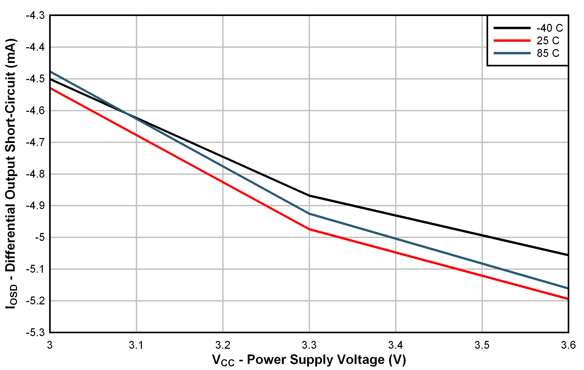
DSLVDS1001 IOSD.pngFigure 4. Differential Output Short-Circuit Current vs Power Supply Voltage
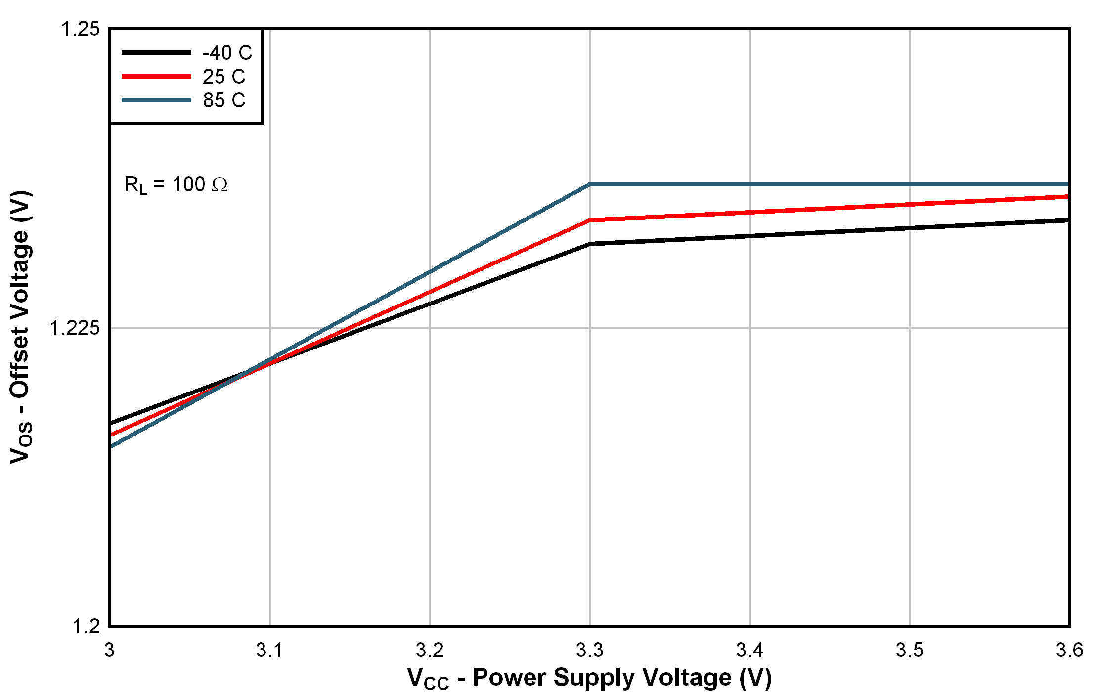
DSLVDS1001 VOS_100OhmLoad.pngFigure 6. Offset Voltage vs Power Supply Voltage